Table of Contents
- 1. Product Overview
- 2. In-Depth Technical Parameter Analysis
- 2.1 Absolute Maximum Ratings
- 2.2 Electro-Optical Characteristics
- 3. Binning System Explanation
- 3.1 Luminous Intensity Binning
- 3.2 Forward Voltage Binning
- 3.3 Color Binning
- 4. Performance Curve Analysis
- 5. Mechanical and Package Information
- 6. Soldering and Assembly Guidelines
- 7. Packaging and Ordering Information
- 8. Application Suggestions and Design Considerations
- 9. Technical Comparison and Differentiation
- 10. Frequently Asked Questions (Based on Technical Parameters)
- 11. Practical Design and Usage Case
- 12. Operating Principle Introduction
- 13. Technology Trends and Context
- LED Specification Terminology
- Photoelectric Performance
- Electrical Parameters
- Thermal Management & Reliability
- Packaging & Materials
- Quality Control & Binning
- Testing & Certification
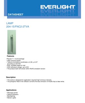
1. Product Overview
This document details the specifications for a high-luminosity white light-emitting diode (LED) encapsulated in a standard T-1 (3mm) round package. The device is engineered to deliver superior luminous output, making it suitable for applications requiring bright, clear indicators or illumination. The white light is generated by a blue InGaN semiconductor chip, the emission of which is converted to white light by a phosphor layer deposited within the reflector cup. This design approach allows for efficient and consistent white light production.
The core advantages of this LED include its high luminous intensity, which can reach up to 14,250 millicandelas (mcd) under standard test conditions. It features a popular and widely compatible package form factor, ensuring ease of integration into existing designs and manufacturing processes. The device is compliant with relevant environmental regulations and offers robust electrostatic discharge (ESD) protection, enhancing its reliability in various handling and operational environments.
The target market for this component spans a broad range of electronic applications. Its primary uses include serving as optical indicators on control panels and instrumentation, providing backlighting for small displays or legends, functioning as marker or status lights, and being integrated into message panels or signage where high visibility is paramount.
2. In-Depth Technical Parameter Analysis
2.1 Absolute Maximum Ratings
The absolute maximum ratings define the stress limits beyond which permanent damage to the device may occur. These values should never be exceeded, even momentarily, in circuit design.
- Continuous Forward Current (IF): 30 mA. This is the maximum DC current that can be continuously applied to the LED anode.
- Peak Forward Current (IFP): 100 mA. This pulsed current rating (at 1/10 duty cycle, 1 kHz) is relevant for multiplexing or PWM dimming applications.
- Reverse Voltage (VR): 5 V. Applying a reverse bias voltage exceeding this limit can cause immediate junction breakdown.
- Power Dissipation (Pd): 110 mW. This is the maximum allowable power loss within the device, calculated as the product of forward voltage and current, plus any minor reverse leakage.
- Operating & Storage Temperature: The device is rated for operation from -40°C to +85°C and can be stored from -40°C to +100°C.
- ESD Withstand (HBM): 4 kV. This Human Body Model rating indicates a good level of protection against electrostatic discharge during handling.
- Soldering Temperature: The leads can withstand 260°C for 5 seconds, which is compatible with standard wave or reflow soldering processes.
2.2 Electro-Optical Characteristics
These parameters are measured under standard test conditions (Ta = 25°C) and represent the typical performance of the device.
- Forward Voltage (VF): 2.8 V to 3.6 V at IF = 20 mA. The typical value is around 3.2V. This range is critical for designing the current-limiting circuitry.
- Luminous Intensity (IV): 7,150 mcd to 14,250 mcd at IF = 20 mA. This high intensity is a key feature, with the actual value determined by the bin code (see Section 3).
- Viewing Angle (2θ1/2): Approximately 25 degrees. This narrow viewing angle concentrates the light output into a focused beam, contributing to the high axial intensity.
- Chromaticity Coordinates: Typical coordinates are x=0.26, y=0.27 on the CIE 1931 color space diagram. This defines the white point of the emitted light.
- Reverse Current (IR): Maximum 50 µA at VR = 5V, indicating very low leakage in the off-state.
3. Binning System Explanation
To ensure consistency in mass production, LEDs are sorted into bins based on key performance parameters. This allows designers to select parts that meet specific requirements for brightness and forward voltage.
3.1 Luminous Intensity Binning
The luminous output is categorized into three primary bins, designated by the codes T, U, and V. Each bin has a defined minimum and maximum intensity measured at 20mA.
- Bin T: 7,150 mcd (Min) to 9,000 mcd (Max)
- Bin U: 9,000 mcd (Min) to 11,250 mcd (Max)
- Bin V: 11,250 mcd (Min) to 14,250 mcd (Max)
A general tolerance of ±10% applies to the luminous intensity within each bin.
3.2 Forward Voltage Binning
The forward voltage drop is sorted into four bins, coded 0 through 3. This is crucial for ensuring uniform brightness when multiple LEDs are connected in parallel or when designing precise driver circuits.
- Bin 0: 2.8 V to 3.0 V
- Bin 1: 3.0 V to 3.2 V
- Bin 2: 3.2 V to 3.4 V
- Bin 3: 3.4 V to 3.6 V
The measurement uncertainty for forward voltage is ±0.1V.
3.3 Color Binning
The white color point is controlled within specific regions on the CIE chromaticity diagram. The datasheet defines two primary color ranks, A0 and A1, each with a quadrilateral boundary defined by four (x,y) coordinate pairs. The typical chromaticity (x=0.26, y=0.27) falls within these defined regions. The measurement uncertainty for color coordinates is ±0.01. The product is supplied in a combined bin group (2) which includes LEDs from both the A1 and A0 color ranks.
4. Performance Curve Analysis
The provided characteristic curves offer deeper insight into the device's behavior under varying conditions.
- Relative Intensity vs. Wavelength: This curve shows the spectral power distribution of the emitted white light. It typically features a primary peak in the blue region (from the InGaN chip) and a broader secondary peak in the yellow-green region (from the phosphor), combining to create white light.
- Directivity Pattern: The polar diagram illustrates the spatial distribution of light intensity, confirming the approximately 25-degree viewing angle where intensity falls to half its axial value.
- Forward Current vs. Forward Voltage (I-V Curve): This exponential curve is fundamental for driver design. It shows the relationship between applied voltage and resulting current, highlighting the need for current-limiting solutions, not voltage sources, to drive LEDs.
- Relative Intensity vs. Forward Current: This curve demonstrates how light output increases with drive current. It is generally linear within the recommended operating range but will saturate at higher currents due to thermal and efficiency effects.
- Chromaticity vs. Forward Current: This plot shows how the white point (color coordinates) may shift slightly with changes in drive current, which is important for color-critical applications.
- Forward Current vs. Ambient Temperature: This derating curve indicates how the maximum safe operating current decreases as the ambient temperature rises, essential for ensuring long-term reliability in high-temperature environments.
5. Mechanical and Package Information
The device uses a standard T-1 (3mm diameter) round package with a water-clear resin lens. Key mechanical dimensions include the overall package diameter, the height from the seating plane to the top of the lens, and the lead spacing. The leadframe is designed for through-hole mounting. The anode and cathode are identified by lead length or other physical markers (typically, the longer lead is the anode). A detailed dimensioned drawing specifies all critical measurements, including lead diameter, seating plane position, and any protrusions. Notes specify that all dimensions are in millimeters with a standard tolerance of ±0.25mm unless otherwise stated, and lead spacing is measured at the point where the lead exits the package body.
6. Soldering and Assembly Guidelines
Proper handling is critical to maintaining LED performance and reliability.
- Lead Forming: Bends must be made at least 3mm from the base of the epoxy lens to avoid stress cracks. Forming must be done before soldering and at room temperature. PCB holes must align perfectly with LED leads to avoid mounting stress.
- Storage: LEDs should be stored at ≤30°C and ≤70% RH. The shelf life from shipment is 3 months. For longer storage (up to 1 year), use a sealed, nitrogen-filled container with desiccant. Avoid rapid temperature changes in humid environments to prevent condensation.
- Soldering: Maintain a minimum distance of 3mm from the solder joint to the epoxy bulb. Recommended conditions are:
Hand Soldering: Iron tip ≤300°C, time ≤3 seconds.
Wave Soldering: Preheat ≤100°C (≤60s), solder bath ≤260°C for ≤5 seconds.
Avoid mechanical stress on the leads during and immediately after soldering while the package is hot.
7. Packaging and Ordering Information
The LEDs are supplied in moisture-resistant, anti-static packaging to protect them from ESD and environmental damage during shipping and storage. The packing specification typically involves placing the LEDs in anti-static bags, which are then packed into inner cartons, which are subsequently packed into master shipping cartons. A standard packing quantity is 200-1000 pieces per bag, 5 bags per inner carton, and 10 inner cartons per outside carton. The product label includes critical information for traceability and identification: Customer Part Number (CPN), Manufacturer Part Number (P/N), Quantity (QTY), combined rank for Luminous Intensity and Forward Voltage (CAT), Color Rank (HUE), Reference (REF), and Lot Number (LOT No.). The product designation follows a specific format (e.g., 204-15/FNC2-2TVA) which encodes the product family and its specific bin selections for intensity, voltage, and color.
8. Application Suggestions and Design Considerations
Typical Application Scenarios: This high-intensity LED is ideal for panel indicator lights where visibility is crucial, even in well-lit conditions. It serves excellently as a backlight for small switches, keypads, or translucent panels. Its use in marker lights for equipment status or emergency indicators is another key application. In message panels or low-resolution dot-matrix displays, it provides bright, discrete pixels.
Design Considerations:
- Current Driving: Always use a constant current driver or a current-limiting resistor in series with a voltage source. Calculate the resistor value using R = (Vsupply - VF) / IF, where VF should be chosen from the maximum bin value (3.6V) for a robust design.
- Thermal Management: While the power dissipation is low, ensuring adequate ventilation and avoiding placement near other heat sources will maintain light output and longevity, especially at higher drive currents or elevated ambient temperatures.
- Optical Design: The narrow viewing angle creates a spotlight effect. For wider illumination, secondary optics like diffusers or lenses may be required.
- ESD Precautions: Although rated for 4kV HBM, standard ESD handling procedures (grounded workstations, wrist straps) are recommended during assembly.
9. Technical Comparison and Differentiation
Compared to generic 3mm white LEDs, this device differentiates itself primarily through its exceptionally high luminous intensity, which can be over twice that of standard parts. The formal binning system for intensity, voltage, and color provides a level of consistency and predictability that is essential for professional and high-volume applications where uniform appearance and performance are required. The inclusion of comprehensive maximum ratings, characteristic curves, and detailed handling instructions indicates a product designed for reliability and ease of integration into demanding applications, setting it apart from basic commodity LEDs.
10. Frequently Asked Questions (Based on Technical Parameters)
Q: What resistor do I need for a 5V supply?
A: Using the maximum VF of 3.6V and a target IF of 20mA: R = (5V - 3.6V) / 0.02A = 70 Ohms. Use the nearest standard value (e.g., 68 or 75 Ohms) and check the actual current and power rating of the resistor.
Q: Can I drive this LED at 30mA continuously?
A: Yes, 30mA is within the absolute maximum continuous current rating. However, operating at the maximum rating may reduce lifetime and increase junction temperature. For optimal longevity, driving at 20mA or lower is recommended.
Q: How do I identify the anode and cathode?
A: Typically, the longer lead is the anode (+). Additionally, the cathode side of the LED package may have a flat edge or other marking on the flange. Always verify with the datasheet diagram.
Q: Why is my LED dimmer than expected?
A: Possible causes include: driving at a current lower than 20mA, using a forward voltage value for calculation that is too high (causing lower actual current), being in a lower intensity bin (T vs. V), or significant junction temperature rise due to poor heat sinking or high ambient temperature.
11. Practical Design and Usage Case
Case: Designing a High-Visibility Status Indicator Panel
An industrial control panel requires a set of status indicators (Power On, System Active, Fault) that must be clearly visible from a distance of 10 meters in a brightly lit factory environment. Using this high-intensity LED is an ideal solution. The designer would select LEDs from the highest luminous intensity bin (V) to ensure maximum brightness. To ensure uniform appearance, they would also specify a tight forward voltage bin (e.g., Bin 1: 3.0-3.2V) and a single color rank (A0 or A1). The LEDs would be driven at 20mA via a constant-current driver circuit shared across all indicators to guarantee identical current and therefore identical brightness. The narrow viewing angle helps concentrate the light toward the operator's line of sight. The 4kV ESD rating provides added robustness for an industrial setting.
12. Operating Principle Introduction
This LED operates on the principle of electroluminescence in a semiconductor p-n junction. When a forward voltage exceeding the junction's built-in potential is applied, electrons from the n-type region and holes from the p-type region are injected into the active region where they recombine. In this specific device, the active region is composed of Indium Gallium Nitride (InGaN), which emits photons in the blue spectrum upon recombination. This blue light is not emitted directly. Instead, it strikes a phosphor coating (typically Yttrium Aluminum Garnet doped with Cerium, or YAG:Ce) deposited inside the reflector cup surrounding the chip. The phosphor absorbs the high-energy blue photons and re-emits lower-energy photons across a broad spectrum, primarily in the yellow range. The combination of the remaining blue light and the converted yellow light is perceived by the human eye as white light. This method is known as phosphor-converted white LED technology.
13. Technology Trends and Context
The use of InGaN-based blue chips with phosphor conversion represents the dominant technology for producing white LEDs for general lighting and indicators. The trend in this field is continuously towards higher luminous efficacy (more lumens per watt), improved color rendering index (CRI) for better color accuracy, and greater consistency in color point and brightness (tighter binning). While this datasheet describes a through-hole package, the broader industry trend is strongly towards surface-mount device (SMD) packages like 3528, 5050, or 2835 for most new designs due to their smaller size, better thermal path to the PCB, and suitability for automated assembly. However, T-1 and other through-hole packages remain vital for applications requiring high single-point intensity, extreme robustness, manual assembly, or legacy system maintenance. Advances in phosphor technology and chip design continue to push the performance boundaries of all LED form factors.
LED Specification Terminology
Complete explanation of LED technical terms
Photoelectric Performance
| Term | Unit/Representation | Simple Explanation | Why Important |
|---|---|---|---|
| Luminous Efficacy | lm/W (lumens per watt) | Light output per watt of electricity, higher means more energy efficient. | Directly determines energy efficiency grade and electricity cost. |
| Luminous Flux | lm (lumens) | Total light emitted by source, commonly called "brightness". | Determines if the light is bright enough. |
| Viewing Angle | ° (degrees), e.g., 120° | Angle where light intensity drops to half, determines beam width. | Affects illumination range and uniformity. |
| CCT (Color Temperature) | K (Kelvin), e.g., 2700K/6500K | Warmth/coolness of light, lower values yellowish/warm, higher whitish/cool. | Determines lighting atmosphere and suitable scenarios. |
| CRI / Ra | Unitless, 0–100 | Ability to render object colors accurately, Ra≥80 is good. | Affects color authenticity, used in high-demand places like malls, museums. |
| SDCM | MacAdam ellipse steps, e.g., "5-step" | Color consistency metric, smaller steps mean more consistent color. | Ensures uniform color across same batch of LEDs. |
| Dominant Wavelength | nm (nanometers), e.g., 620nm (red) | Wavelength corresponding to color of colored LEDs. | Determines hue of red, yellow, green monochrome LEDs. |
| Spectral Distribution | Wavelength vs intensity curve | Shows intensity distribution across wavelengths. | Affects color rendering and quality. |
Electrical Parameters
| Term | Symbol | Simple Explanation | Design Considerations |
|---|---|---|---|
| Forward Voltage | Vf | Minimum voltage to turn on LED, like "starting threshold". | Driver voltage must be ≥Vf, voltages add up for series LEDs. |
| Forward Current | If | Current value for normal LED operation. | Usually constant current drive, current determines brightness & lifespan. |
| Max Pulse Current | Ifp | Peak current tolerable for short periods, used for dimming or flashing. | Pulse width & duty cycle must be strictly controlled to avoid damage. |
| Reverse Voltage | Vr | Max reverse voltage LED can withstand, beyond may cause breakdown. | Circuit must prevent reverse connection or voltage spikes. |
| Thermal Resistance | Rth (°C/W) | Resistance to heat transfer from chip to solder, lower is better. | High thermal resistance requires stronger heat dissipation. |
| ESD Immunity | V (HBM), e.g., 1000V | Ability to withstand electrostatic discharge, higher means less vulnerable. | Anti-static measures needed in production, especially for sensitive LEDs. |
Thermal Management & Reliability
| Term | Key Metric | Simple Explanation | Impact |
|---|---|---|---|
| Junction Temperature | Tj (°C) | Actual operating temperature inside LED chip. | Every 10°C reduction may double lifespan; too high causes light decay, color shift. |
| Lumen Depreciation | L70 / L80 (hours) | Time for brightness to drop to 70% or 80% of initial. | Directly defines LED "service life". |
| Lumen Maintenance | % (e.g., 70%) | Percentage of brightness retained after time. | Indicates brightness retention over long-term use. |
| Color Shift | Δu′v′ or MacAdam ellipse | Degree of color change during use. | Affects color consistency in lighting scenes. |
| Thermal Aging | Material degradation | Deterioration due to long-term high temperature. | May cause brightness drop, color change, or open-circuit failure. |
Packaging & Materials
| Term | Common Types | Simple Explanation | Features & Applications |
|---|---|---|---|
| Package Type | EMC, PPA, Ceramic | Housing material protecting chip, providing optical/thermal interface. | EMC: good heat resistance, low cost; Ceramic: better heat dissipation, longer life. |
| Chip Structure | Front, Flip Chip | Chip electrode arrangement. | Flip chip: better heat dissipation, higher efficacy, for high-power. |
| Phosphor Coating | YAG, Silicate, Nitride | Covers blue chip, converts some to yellow/red, mixes to white. | Different phosphors affect efficacy, CCT, and CRI. |
| Lens/Optics | Flat, Microlens, TIR | Optical structure on surface controlling light distribution. | Determines viewing angle and light distribution curve. |
Quality Control & Binning
| Term | Binning Content | Simple Explanation | Purpose |
|---|---|---|---|
| Luminous Flux Bin | Code e.g., 2G, 2H | Grouped by brightness, each group has min/max lumen values. | Ensures uniform brightness in same batch. |
| Voltage Bin | Code e.g., 6W, 6X | Grouped by forward voltage range. | Facilitates driver matching, improves system efficiency. |
| Color Bin | 5-step MacAdam ellipse | Grouped by color coordinates, ensuring tight range. | Guarantees color consistency, avoids uneven color within fixture. |
| CCT Bin | 2700K, 3000K etc. | Grouped by CCT, each has corresponding coordinate range. | Meets different scene CCT requirements. |
Testing & Certification
| Term | Standard/Test | Simple Explanation | Significance |
|---|---|---|---|
| LM-80 | Lumen maintenance test | Long-term lighting at constant temperature, recording brightness decay. | Used to estimate LED life (with TM-21). |
| TM-21 | Life estimation standard | Estimates life under actual conditions based on LM-80 data. | Provides scientific life prediction. |
| IESNA | Illuminating Engineering Society | Covers optical, electrical, thermal test methods. | Industry-recognized test basis. |
| RoHS / REACH | Environmental certification | Ensures no harmful substances (lead, mercury). | Market access requirement internationally. |
| ENERGY STAR / DLC | Energy efficiency certification | Energy efficiency and performance certification for lighting. | Used in government procurement, subsidy programs, enhances competitiveness. |