Table of Contents
- 1. Product Overview
- 2. In-Depth Technical Parameter Analysis
- 2.1 Absolute Maximum Ratings
- 2.2 Electrical Characteristics
- 2.3 Thermal Characteristics
- 3. Performance Curve Analysis
- 3.1 VF-IF Characteristics
- 3.2 VR-IR Characteristics
- 3.3 Maximum Forward Current vs. Case Temperature
- 3.4 Power Dissipation vs. Case Temperature
- 3.5 Transient Thermal Impedance
- 4. Mechanical and Package Information
- 4.1 Package Outline and Dimensions
- 4.2 Pin Configuration and Polarity
- 4.3 Recommended PCB Pad Layout
- 5. Soldering and Assembly Guidelines
- 6. Application Recommendations
- 6.1 Typical Application Circuits
- 6.2 Design Considerations
- 7. Technical Comparison and Advantages
- 8. Frequently Asked Questions (FAQs)
- 9. Design and Usage Case Study
- 10. Operating Principle
- 11. Technology Trends
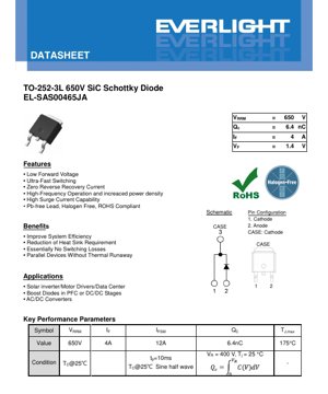
1. Product Overview
This document details the specifications for a high-performance Silicon Carbide (SiC) Schottky Barrier Diode (SBD) in a surface-mount TO-252-3L package, commonly known as DPAK. The device is engineered for high-voltage, high-frequency, and high-efficiency power conversion applications. Its core advantage lies in the fundamental properties of SiC material, which enable superior switching performance and thermal stability compared to traditional silicon-based diodes.
The primary target markets for this component include modern power supply designs, renewable energy systems like solar inverters, motor drive circuits, and data center power infrastructure. It is specifically suited for applications demanding minimal switching losses and high power density.
2. In-Depth Technical Parameter Analysis
2.1 Absolute Maximum Ratings
The device is rated for a repetitive peak reverse voltage (VRRM) of 650V, with a matching DC blocking voltage (VR). The maximum continuous forward current (IF) is 4A, limited by thermal considerations. A key robustness parameter is the non-repetitive surge current (IFSM) of 12A for a 10ms half-sine wave pulse, indicating its ability to handle short-circuit or inrush current conditions. The maximum junction temperature (TJ) is 175°C, defining the upper operational limit.
2.2 Electrical Characteristics
The forward voltage (VF) is a critical parameter for conduction losses. At the rated current of 4A and a junction temperature of 25°C, the typical VF is 1.4V, with a maximum of 1.75V. This low value contributes directly to higher system efficiency. The reverse leakage current (IR) is exceptionally low, typically 1µA at 520V and 25°C, minimizing off-state power dissipation.
A defining feature of SiC Schottky diodes is the absence of reverse recovery charge, as indicated by the "Zero Reverse Recovery Current" claim. Instead, the switching behavior is characterized by capacitive charge. The total capacitive charge (QC) is specified as 6.4nC at 400V. This parameter, along with the total capacitance (Ct) which decreases with increasing reverse voltage (e.g., 12pF at 200V, 10pF at 400V), is crucial for calculating capacitive switching losses in high-frequency circuits.
2.3 Thermal Characteristics
The thermal resistance from junction to case (RθJC) is 5.9°C/W (typical). This low value is essential for effective heat transfer from the semiconductor die to the PCB or heatsink. The maximum total power dissipation (PD) is 25W, but practical limits are determined by the application's thermal management and ambient conditions.
3. Performance Curve Analysis
The datasheet includes several typical performance graphs which are vital for design engineers.
3.1 VF-IF Characteristics
This graph shows the relationship between forward voltage and forward current at different junction temperatures. It illustrates how VF has a negative temperature coefficient, decreasing slightly as temperature increases, which is a characteristic of Schottky diodes.
3.2 VR-IR Characteristics
This curve plots reverse leakage current against reverse voltage, typically showing an exponential increase in IR with both increasing voltage and temperature, highlighting the importance of voltage derating at high temperatures.
3.3 Maximum Forward Current vs. Case Temperature
This derating curve is critical for determining the maximum allowable continuous current based on the operating case temperature (TC). It ensures the junction temperature does not exceed its maximum rating.
3.4 Power Dissipation vs. Case Temperature
Similar to the current derating, this graph shows how the maximum permissible power dissipation decreases as the case temperature rises.
3.5 Transient Thermal Impedance
This graph is essential for evaluating the diode's thermal response to short power pulses. It shows the effective thermal resistance from junction to case as a function of pulse width, allowing accurate calculation of peak junction temperature during switching events.
4. Mechanical and Package Information
4.1 Package Outline and Dimensions
The device uses the TO-252-3L (DPAK) package. Key dimensions include an overall package height (H) of 9.84mm (typ), length (E) of 6.60mm (typ), and width (D) of 6.10mm (typ). The lead pitch (e) is 2.28mm (basic). Detailed mechanical drawings with minimum, typical, and maximum values for all critical dimensions are provided to ensure proper PCB footprint design and assembly clearance.
4.2 Pin Configuration and Polarity
The pinout is clearly defined: Pin 1 is the Cathode, Pin 2 is the Anode, and the metal tab (Case) is connected to the Cathode. Correct polarity identification is crucial to prevent device failure during installation.
4.3 Recommended PCB Pad Layout
A suggested surface-mount pad layout is included to optimize solder joint reliability and thermal performance. Following this layout helps in achieving proper solder fillets and effective heat sinking through the exposed metal tab.
5. Soldering and Assembly Guidelines
While specific reflow profiles are not detailed in the provided excerpt, standard IPC/JEDEC guidelines for surface-mount assembly of lead-free components should be followed. The device is specified as Pb-free and Halogen Free, compliant with RoHS directives. Care must be taken during handling to avoid mechanical stress on the leads. Storage should be in a dry, controlled environment to prevent moisture absorption, which could lead to "popcorning" during reflow soldering.
6. Application Recommendations
6.1 Typical Application Circuits
This diode is ideally suited for use as a boost diode in Power Factor Correction (PFC) stages, freewheeling diode in bridge circuits, and output rectifier in high-frequency AC/DC or DC/DC converters. Its fast switching capability makes it excellent for circuits operating in the tens to hundreds of kilohertz range.
6.2 Design Considerations
- Switching Losses: While reverse recovery loss is negligible, capacitive switching loss (proportional to QC * V^2 * f) becomes significant at very high frequencies and voltages. This must be calculated.
- Thermal Management: The low RθJC allows efficient heat transfer. A sufficiently large copper area on the PCB connected to the cathode tab is necessary to act as a heatsink. Thermal vias can be used to transfer heat to inner or bottom layers.
- Paralleling Devices: The positive temperature coefficient of VF facilitates current sharing when multiple diodes are connected in parallel, reducing the risk of thermal runaway.
- Voltage Spikes: In inductive switching circuits, proper snubber design or careful layout is required to manage voltage overshoot and prevent exceeding the VRRM rating.
7. Technical Comparison and Advantages
Compared to silicon PN junction fast recovery diodes (FRDs) or even silicon Schottky diodes, this SiC Schottky diode offers distinct advantages:
- Zero Reverse Recovery: Eliminates a major source of switching loss and EMI in silicon FRDs, enabling higher efficiency and frequency.
- Higher Operating Temperature: A TJ,max of 175°C vs. typically 150°C for many silicon devices, allowing for more compact designs or higher ambient temperature operation.
- Higher Voltage Rating: Silicon Schottky diodes are typically limited to below 200V. This 650V rating opens up use in mainstream offline power supplies.
- Lower Forward Voltage at High Temperature: The VF of SiC Schottky diodes remains relatively stable or even decreases with temperature, unlike silicon diodes where it increases, leading to better performance under hot conditions.
8. Frequently Asked Questions (FAQs)
Q: What does "Zero Reverse Recovery Current" mean in practice?
A: It means when the diode switches from conducting to blocking, there is no stored minority carrier charge that needs to be removed (recovered). The current stops almost instantly, eliminating the reverse recovery current spike and associated power loss seen in standard PN diodes.
Q: How do I calculate the switching losses for this diode?
A: For this capacitive-switching device, the dominant dynamic loss is the energy required to charge its junction capacitance each cycle. The loss per cycle can be approximated as 0.5 * C(VR) * VR^2, where C(VR) is the voltage-dependent capacitance. Multiply by switching frequency (f) to get power loss: P_sw ≈ 0.5 * C(VR) * VR^2 * f. The QC parameter provides another method for loss estimation.
Q: Can I use this diode to replace a silicon ultra-fast diode directly?
A: Electrically, in many cases, yes, and it will likely improve efficiency. However, you must verify the layout and thermal design are adequate, as the switching behavior (capacitive vs. recovery) is different and may affect voltage ringing. Also, ensure the gate drive for any associated switching transistor is robust enough to handle potentially different switching dynamics.
Q: Why is the surge current rating important?
A: It indicates the diode's ability to withstand unexpected fault conditions, such as the initial inrush current when charging a large capacitor at power-up, or a temporary short-circuit event. This adds a layer of robustness to the design.
9. Design and Usage Case Study
Scenario: Designing a 1kW Totem-Pole PFC Stage.
In a modern bridgeless totem-pole PFC circuit operating at 100kHz, the traditional silicon boost diode is a major source of loss. Replacing it with this 650V SiC Schottky diode would yield significant benefits. The zero reverse recovery eliminates the turn-on loss in the complementary MOSFET that occurs when the diode's recovery current is commutated. This allows for higher frequency operation, reducing the size of the magnetic components (inductor). The low forward voltage reduces conduction loss. The designer must carefully model the capacitive turn-off loss of the SiC diode at 400V DC bus voltage and 100kHz to ensure it is acceptable, and design the PCB with a large, thick copper pour attached to the diode's tab to manage the ~3-4W of estimated conduction loss.
10. Operating Principle
A Schottky diode is formed by a metal-semiconductor junction, rather than a PN semiconductor junction. This metal-SiC junction creates a Schottky barrier which allows for majority carrier conduction only (electrons in an N-type SiC substrate). When forward biased, electrons have enough energy to cross the barrier, enabling current flow. When reverse biased, the barrier widens, blocking current. The absence of minority carrier injection and storage is the fundamental reason for the ultra-fast switching and lack of reverse recovery. Silicon Carbide's wide bandgap provides the material with high critical electric field strength, enabling thinner drift layers and thus lower on-resistance and capacitance for a given voltage rating compared to silicon.
11. Technology Trends
Silicon Carbide power devices are a key enabling technology for the evolution towards more efficient and compact power electronics. Trends include increasing voltage ratings (towards 1.2kV and 1.7kV for automotive and industrial drives), higher current density in smaller packages, and the integration of SiC Schottky diodes with SiC MOSFETs in co-packaged modules. As manufacturing volumes increase and costs decrease, SiC is moving from niche applications into mainstream consumer, industrial, and automotive power supplies, driven by global demands for energy efficiency and electrification. The development focuses on improving wafer quality, reducing defect densities, and optimizing device structures to further lower specific on-resistance and capacitance.
LED Specification Terminology
Complete explanation of LED technical terms
Photoelectric Performance
| Term | Unit/Representation | Simple Explanation | Why Important |
|---|---|---|---|
| Luminous Efficacy | lm/W (lumens per watt) | Light output per watt of electricity, higher means more energy efficient. | Directly determines energy efficiency grade and electricity cost. |
| Luminous Flux | lm (lumens) | Total light emitted by source, commonly called "brightness". | Determines if the light is bright enough. |
| Viewing Angle | ° (degrees), e.g., 120° | Angle where light intensity drops to half, determines beam width. | Affects illumination range and uniformity. |
| CCT (Color Temperature) | K (Kelvin), e.g., 2700K/6500K | Warmth/coolness of light, lower values yellowish/warm, higher whitish/cool. | Determines lighting atmosphere and suitable scenarios. |
| CRI / Ra | Unitless, 0–100 | Ability to render object colors accurately, Ra≥80 is good. | Affects color authenticity, used in high-demand places like malls, museums. |
| SDCM | MacAdam ellipse steps, e.g., "5-step" | Color consistency metric, smaller steps mean more consistent color. | Ensures uniform color across same batch of LEDs. |
| Dominant Wavelength | nm (nanometers), e.g., 620nm (red) | Wavelength corresponding to color of colored LEDs. | Determines hue of red, yellow, green monochrome LEDs. |
| Spectral Distribution | Wavelength vs intensity curve | Shows intensity distribution across wavelengths. | Affects color rendering and quality. |
Electrical Parameters
| Term | Symbol | Simple Explanation | Design Considerations |
|---|---|---|---|
| Forward Voltage | Vf | Minimum voltage to turn on LED, like "starting threshold". | Driver voltage must be ≥Vf, voltages add up for series LEDs. |
| Forward Current | If | Current value for normal LED operation. | Usually constant current drive, current determines brightness & lifespan. |
| Max Pulse Current | Ifp | Peak current tolerable for short periods, used for dimming or flashing. | Pulse width & duty cycle must be strictly controlled to avoid damage. |
| Reverse Voltage | Vr | Max reverse voltage LED can withstand, beyond may cause breakdown. | Circuit must prevent reverse connection or voltage spikes. |
| Thermal Resistance | Rth (°C/W) | Resistance to heat transfer from chip to solder, lower is better. | High thermal resistance requires stronger heat dissipation. |
| ESD Immunity | V (HBM), e.g., 1000V | Ability to withstand electrostatic discharge, higher means less vulnerable. | Anti-static measures needed in production, especially for sensitive LEDs. |
Thermal Management & Reliability
| Term | Key Metric | Simple Explanation | Impact |
|---|---|---|---|
| Junction Temperature | Tj (°C) | Actual operating temperature inside LED chip. | Every 10°C reduction may double lifespan; too high causes light decay, color shift. |
| Lumen Depreciation | L70 / L80 (hours) | Time for brightness to drop to 70% or 80% of initial. | Directly defines LED "service life". |
| Lumen Maintenance | % (e.g., 70%) | Percentage of brightness retained after time. | Indicates brightness retention over long-term use. |
| Color Shift | Δu′v′ or MacAdam ellipse | Degree of color change during use. | Affects color consistency in lighting scenes. |
| Thermal Aging | Material degradation | Deterioration due to long-term high temperature. | May cause brightness drop, color change, or open-circuit failure. |
Packaging & Materials
| Term | Common Types | Simple Explanation | Features & Applications |
|---|---|---|---|
| Package Type | EMC, PPA, Ceramic | Housing material protecting chip, providing optical/thermal interface. | EMC: good heat resistance, low cost; Ceramic: better heat dissipation, longer life. |
| Chip Structure | Front, Flip Chip | Chip electrode arrangement. | Flip chip: better heat dissipation, higher efficacy, for high-power. |
| Phosphor Coating | YAG, Silicate, Nitride | Covers blue chip, converts some to yellow/red, mixes to white. | Different phosphors affect efficacy, CCT, and CRI. |
| Lens/Optics | Flat, Microlens, TIR | Optical structure on surface controlling light distribution. | Determines viewing angle and light distribution curve. |
Quality Control & Binning
| Term | Binning Content | Simple Explanation | Purpose |
|---|---|---|---|
| Luminous Flux Bin | Code e.g., 2G, 2H | Grouped by brightness, each group has min/max lumen values. | Ensures uniform brightness in same batch. |
| Voltage Bin | Code e.g., 6W, 6X | Grouped by forward voltage range. | Facilitates driver matching, improves system efficiency. |
| Color Bin | 5-step MacAdam ellipse | Grouped by color coordinates, ensuring tight range. | Guarantees color consistency, avoids uneven color within fixture. |
| CCT Bin | 2700K, 3000K etc. | Grouped by CCT, each has corresponding coordinate range. | Meets different scene CCT requirements. |
Testing & Certification
| Term | Standard/Test | Simple Explanation | Significance |
|---|---|---|---|
| LM-80 | Lumen maintenance test | Long-term lighting at constant temperature, recording brightness decay. | Used to estimate LED life (with TM-21). |
| TM-21 | Life estimation standard | Estimates life under actual conditions based on LM-80 data. | Provides scientific life prediction. |
| IESNA | Illuminating Engineering Society | Covers optical, electrical, thermal test methods. | Industry-recognized test basis. |
| RoHS / REACH | Environmental certification | Ensures no harmful substances (lead, mercury). | Market access requirement internationally. |
| ENERGY STAR / DLC | Energy efficiency certification | Energy efficiency and performance certification for lighting. | Used in government procurement, subsidy programs, enhances competitiveness. |