Table of Contents
- 1. Product Overview
- 2. Technical Parameter Deep Dive
- 2.1 Absolute Maximum Ratings
- 2.2 Electrical Characteristics
- 2.2.1 Input Characteristics
- 2.2.2 Output & Transfer Characteristics
- 2.3 Switching Characteristics
- 3. Performance Curve Analysis
- 4. Mechanical & Package Information
- 4.1 Pin Configuration
- 5. Soldering & Assembly Guidelines
- 6. Application Suggestions
- 6.1 Typical Application Circuits
- 6.2 Design Considerations
- 7. Technical Comparison & Differentiation
- 8. Frequently Asked Questions (Based on Technical Parameters)
- 9. Operational Principle
- 10. Industry Trends & Context
1. Product Overview
The EL063X series represents a family of dual-channel, high-speed logic gate photocouplers (opto-isolators). These devices are engineered to provide robust electrical isolation and high-speed digital signal transmission between two circuits. The core function is to transfer logic-level signals across an isolation barrier using an infrared light-emitting diode (LED) optically coupled to a high-speed integrated photodetector with a logic gate output. This design effectively breaks ground loops, prevents noise transmission, and protects sensitive circuitry from voltage spikes or differences in ground potential.
The primary application domains for this component are in industrial automation, communication interfaces, power supply control, and computer peripherals where reliable, noise-immune signal transfer is critical. The dual-channel configuration in a single package offers space-saving benefits and matched channel characteristics for differential signal applications or for isolating multiple control lines.
2. Technical Parameter Deep Dive
The electrical and optical parameters define the operational boundaries and performance of the photocoupler.
2.1 Absolute Maximum Ratings
These are stress limits that must not be exceeded under any conditions, even momentarily. Operating the device beyond these ratings may cause permanent damage.
- Input Forward Current (IF): 20 mA DC/average. This limits the maximum current through the input LED.
- Input Reverse Voltage (VR): 5 V. The maximum reverse bias voltage the input LED can withstand.
- Output Current (IO): 50 mA. The maximum current the output transistor can sink.
- Output Voltage (VO) & Supply Voltage (VCC): 7.0 V. The maximum voltage that can be applied to the output side pins.
- Isolation Voltage (VISO): 3750 Vrms for 1 minute. This is a key safety parameter indicating the dielectric strength of the isolation barrier between the input and output sides, tested with pins 1-4 shorted together and pins 5-8 shorted together.
- Operating Temperature (TOPR): -40°C to +100°C. The ambient temperature range over which the device is guaranteed to function.
- Storage Temperature (TSTG): -55°C to +125°C.
2.2 Electrical Characteristics
These parameters are guaranteed over the specified operating conditions (Ta = -40°C to 85°C unless noted).
2.2.1 Input Characteristics
- Forward Voltage (VF): Typically 1.4V, with a maximum of 1.8V at IF = 10 mA. This is used to calculate the required series resistor for the input LED drive circuit.
- Temperature Coefficient of VF: Approximately -1.8 mV/°C. The LED forward voltage decreases as temperature increases.
- Input Capacitance (CIN): Typically 60 pF. This parasitic capacitance affects high-frequency performance on the input side.
2.2.2 Output & Transfer Characteristics
- Supply Current (ICCH/ICCL): The quiescent current drawn by the output IC. ICCH (output high) is typically 13 mA (max 18 mA). ICCL (output low) is typically 15 mA (max 21 mA) at VCC = 5.5V. This is important for power budget calculations.
- High-Level Output Current (IOH): The output can source a maximum of 100 µA while maintaining a high logic level (VO near VCC). This is a weak sourcing capability.
- Low-Level Output Voltage (VOL): Maximum 0.6V at IF = 5mA and ICL = 13mA. This defines the voltage level when the output transistor is actively sinking current, ensuring compatibility with TTL/CMOS logic low thresholds.
- Input Threshold Current (IFT): Maximum 5 mA. This is the input current required to guarantee the output switches to a valid low state (VO ≤ 0.6V) under the specified conditions. Designers must ensure the drive circuit provides at least this current for reliable switching.
2.3 Switching Characteristics
These parameters define the high-speed digital performance, measured under standard test conditions (Ta=25°C, VCC=5V, IF=7.5mA, CL=15pF, RL=350Ω).
- Propagation Delay (tPHL, tPLH): Maximum 100 ns each. tPHL is the delay from the input LED turning ON (current rising) to the output falling. tPLH is the delay from the input LED turning OFF (current falling) to the output rising. These delays limit the maximum data rate.
- Pulse Width Distortion (|tPHL – tPLH|): Maximum 35 ns. This asymmetry between rise and fall delays can distort the duty cycle of transmitted pulses, which is critical in timing-sensitive applications.
- Output Rise/Fall Time (tr, tf): tr is typically 40 ns (10% to 90%), tf is typically 10 ns (90% to 10%). The faster fall time is characteristic of the active pull-down output stage.
- Common-Mode Transient Immunity (CMTI): This is a critical parameter for noise immunity in noisy environments like motor drives or switching power supplies. It measures the device's ability to reject fast voltage transients appearing across the isolation barrier.
- EL0630: Minimum 5000 V/µs.
- EL0631: Minimum 10000 V/µs. This higher CMTI makes the EL0631 suitable for more demanding applications with severe electrical noise.
- The immunity is specified for both the output high (CMH) and output low (CML) states, ensuring the output does not falsely toggle during a transient event.
3. Performance Curve Analysis
While the provided PDF excerpt mentions "Typical Electro-Optical Characteristics Curves," the specific graphs are not included in the text. Typically, such curves for a photocoupler would include:
- Current Transfer Ratio (CTR) vs. Forward Current (IF): Shows the efficiency of the optical coupling (output current / input current) across different drive levels.
- Propagation Delay vs. Forward Current (IF): Illustrates how switching speed varies with LED drive current. Higher IF generally decreases propagation delay.
- Propagation Delay vs. Temperature: Shows the temperature dependence of switching speed.
- Output Saturation Voltage vs. Output Current: Characterizes the output transistor's performance when sinking current.
Designers should consult the complete datasheet with graphs to understand these relationships for optimizing their specific application, such as trading off speed against LED current/power dissipation.
4. Mechanical & Package Information
The device is housed in a standard 8-pin Small Outline Package (SOP or SOIC). This surface-mount package conforms to the common SO8 footprint, facilitating easy PCB layout and assembly.
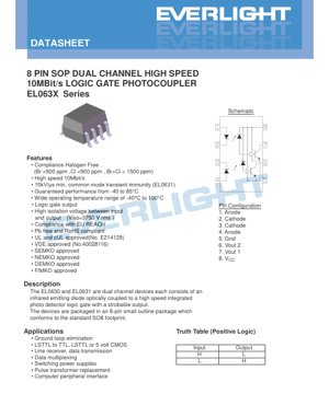
4.1 Pin Configuration
The pinout is as follows:
- Pin 1: Anode (Channel 1 Input LED)
- Pin 2: Cathode (Channel 1 Input LED)
- Pin 3: Cathode (Channel 2 Input LED)
- Pin 4: Anode (Channel 2 Input LED)
- Pin 5: Ground (GND) - Output side common.
- Pin 6: VOUT 2 (Output for Channel 2)
- Pin 7: VOUT 1 (Output for Channel 1)
- Pin 8: VCC (Supply Voltage for Output side, +5V typical)
Important Note: The input and output sides are fully isolated. Pins 1-4 are on the isolated input side, and pins 5-8 are on the isolated output side. The PCB layout must maintain adequate creepage and clearance distances between these two sets of pins and their associated traces to preserve the isolation rating.
5. Soldering & Assembly Guidelines
The device is suitable for standard surface-mount assembly processes.
- Soldering Temperature: The maximum allowable soldering temperature is 260°C for 10 seconds. This is compatible with typical lead-free reflow soldering profiles.
- Moisture Sensitivity: While not explicitly stated in the excerpt, most plastic encapsulated SMDs have a Moisture Sensitivity Level (MSL). Proper handling, baking if required, and storage per manufacturer guidelines are essential to prevent "popcorning" during reflow.
- Output Bypassing: A critical design note (*3) specifies that the VCC supply pin (8) must be bypassed with a 0.1 µF or larger capacitor (ceramic or solid tantalum with good HF characteristics). This capacitor must be placed as close as possible between pin 8 (VCC) and pin 5 (GND) to ensure stable operation and minimize switching noise on the supply rail.
6. Application Suggestions
6.1 Typical Application Circuits
The datasheet lists several key applications:
- Ground Loop Elimination: The primary function, isolating grounds of two subsystems to prevent circulating currents and noise.
- Logic Level Translation/Interface: Can interface between different logic families (e.g., LSTTL to TTL or 5V CMOS) while providing isolation.
- Data Transmission & Line Receivers: Suitable for isolated serial data links (e.g., RS-232, RS-485 isolation), digital I/O isolation, and multiplexing.
- Switching Power Supply Feedback: Isolating the feedback signal from the secondary (output) side to the primary (controller) side in flyback or other isolated converter topologies.
- Pulse Transformer Replacement: Offers a solid-state, potentially more reliable and compact alternative for transmitting digital pulses across an isolation barrier.
- Computer Peripheral Interface: Isolating signals to/from printers, industrial I/O cards, or other peripherals.
6.2 Design Considerations
- Input Drive Circuit: A series resistor must be calculated based on the input supply voltage (VIN), the desired forward current IF, and the LED VF. Rseries = (VIN - VF) / IF. IF must be ≥ IFT for guaranteed switching and can be increased up to the Absolute Maximum Rating to improve speed, at the cost of higher power dissipation.
- Output Load: The output is designed to drive standard logic loads. The pull-up resistor RL (connected between VCC and the output pin) sets the logic high level and the rise time. A smaller RL provides faster rise times but increases power consumption when the output is low. The test condition uses RL=350Ω.
- Power Dissipation: Calculate total power dissipation on both input (PD = VF * IF) and output sides to ensure it remains within limits, especially at high temperatures.
- Channel Selection: Choose EL0631 over EL0630 for applications requiring higher immunity to common-mode noise (CMTI ≥ 10,000 V/µs vs. 5,000 V/µs).
7. Technical Comparison & Differentiation
The EL063X series differentiates itself in the market through several key features:
- High Speed: 10 Mbit/s capability and propagation delays ≤100 ns place it in the high-speed photocoupler category, suitable for fast digital communication.
- Dual Channel in SOP-8: Integrates two isolated channels in a compact, standard package, saving board space compared to two single-channel devices.
- High CMTI: Particularly the EL0631's 10 kV/µs minimum CMTI is a significant advantage in electrically noisy environments like industrial motor drives, where lower-CMTI optocouplers might malfunction.
- Wide Temperature Range: Guaranteed performance from -40°C to 85°C, with an operating range up to 100°C, suits industrial and automotive applications.
- Comprehensive Safety Approvals: The device carries approvals from major international safety agencies (UL, cUL, VDE, SEMKO, etc.), which is often a mandatory requirement for end products in regulated markets.
- Environmental Compliance: It is halogen-free (Br/Cl limits), Pb-free, RoHS compliant, and REACH compliant, meeting modern environmental regulations.
8. Frequently Asked Questions (Based on Technical Parameters)
Q: What is the maximum data rate I can achieve with this photocoupler?
A: The 10 Mbit/s specification and 100 ns max propagation delay suggest a maximum theoretical data rate around 5-10 Mbps for NRZ data. In practice, the achievable rate depends on the specific waveform, rise/fall times, and pulse width distortion. For reliable operation, a conservative design target of 1-5 Mbps is typical.
Q: How do I choose between the EL0630 and EL0631?
A: The primary difference is the Common-Mode Transient Immunity (CMTI). If your application involves significant switching noise (e.g., near motor drives, high-power inverters, noisy power supplies), the EL0631 (10 kV/µs) provides superior noise immunity. For less noisy environments, the EL0630 (5 kV/µs) may be sufficient.
Q: Why is a bypass capacitor required on VCC?
A: The high-speed switching of the output stage can cause instantaneous current spikes on the VCC line. The local bypass capacitor provides a low-impedance source for this current, preventing voltage droops or spikes on VCC that could cause erratic operation or noise radiation. Placing it close to the pins is crucial for effectiveness.
Q: Can I use this device to isolate analog signals?
A: No. This is a logic gate photocoupler. The output is a digital logic level (high or low), not a linear representation of the input current. For analog isolation, a linear optocoupler (with a phototransistor or photodiode output) is required.
Q: What is the purpose of the "strobable output" mentioned in the description?
A> While not detailed in this excerpt, a strobable output typically means the output stage has an enable or strobe control. This allows the output to be turned on/off or latched by a third control signal, which can be useful for multiplexing applications or reducing power consumption. The pin configuration here does not show a separate strobe pin, so this functionality may be integrated internally in a specific mode or may refer to the output being enabled by the input signal itself.
9. Operational Principle
The operational principle is based on optoelectronic conversion. When a sufficient forward current (IF) is applied to the input Infrared Emitting Diode (IRED), it emits light photons. These photons traverse the transparent isolation barrier (typically a molded plastic compound). On the output side, a high-speed silicon photodetector integrated circuit receives this light. This IC contains a photodiode that converts the light back into a photocurrent. This photocurrent is then processed by an internal amplifier and comparator circuit (the "logic gate") to produce a clean, well-defined digital output voltage. When the input LED is ON, the output is driven to a logic LOW state (typically by an active pull-down transistor). When the input LED is OFF, the output circuit pulls the pin to a logic HIGH state (through the external pull-up resistor RL). This positive logic operation is summarized in the provided Truth Table: Input High = Output Low, Input Low = Output High.
10. Industry Trends & Context
The development of photocouplers like the EL063X series is driven by several key trends in electronics:
- Demand for Higher Speed and Bandwidth: As industrial networks (EtherCAT, PROFINET IRT) and communication interfaces speed up, isolators must keep pace. The move from kilobit to megabit and now towards 10+ megabit speeds is evident.
- Increased Noise Immunity Industrial and automotive environments are becoming more electrically complex, necessitating isolators with higher CMTI ratings to ensure reliable operation amidst noise from motor drives, switching power supplies, and RF sources.
- Miniaturization and Integration The dual-channel design in an SOP-8 package reflects the need to save PCB real estate and reduce component count. Further trends include integrating more channels (quad isolators) or combining isolation with other functions like ADC drivers or I2C level translation.
- Enhanced Safety and Reliability Standards Stricter safety regulations across industries push for components with higher isolation voltages, longer operational lifetimes, and robust certifications from agencies like UL, VDE, and CQC.
- Alternative Isolation Technologies While optocouplers are mature, they face competition from capacitive isolators (using SiO2 barriers) and magnetic (giant magnetoresistance or transformer-based) isolators, which can offer advantages in speed, power consumption, and integration density. However, optocouplers maintain strong positions due to their high CMTI, simplicity, and well-understood reliability.
The EL063X series, with its balance of speed, dual-channel integration, high CMTI, and safety certifications, is positioned to address these ongoing demands in the market for robust, high-performance signal isolation.
LED Specification Terminology
Complete explanation of LED technical terms
Photoelectric Performance
| Term | Unit/Representation | Simple Explanation | Why Important |
|---|---|---|---|
| Luminous Efficacy | lm/W (lumens per watt) | Light output per watt of electricity, higher means more energy efficient. | Directly determines energy efficiency grade and electricity cost. |
| Luminous Flux | lm (lumens) | Total light emitted by source, commonly called "brightness". | Determines if the light is bright enough. |
| Viewing Angle | ° (degrees), e.g., 120° | Angle where light intensity drops to half, determines beam width. | Affects illumination range and uniformity. |
| CCT (Color Temperature) | K (Kelvin), e.g., 2700K/6500K | Warmth/coolness of light, lower values yellowish/warm, higher whitish/cool. | Determines lighting atmosphere and suitable scenarios. |
| CRI / Ra | Unitless, 0–100 | Ability to render object colors accurately, Ra≥80 is good. | Affects color authenticity, used in high-demand places like malls, museums. |
| SDCM | MacAdam ellipse steps, e.g., "5-step" | Color consistency metric, smaller steps mean more consistent color. | Ensures uniform color across same batch of LEDs. |
| Dominant Wavelength | nm (nanometers), e.g., 620nm (red) | Wavelength corresponding to color of colored LEDs. | Determines hue of red, yellow, green monochrome LEDs. |
| Spectral Distribution | Wavelength vs intensity curve | Shows intensity distribution across wavelengths. | Affects color rendering and quality. |
Electrical Parameters
| Term | Symbol | Simple Explanation | Design Considerations |
|---|---|---|---|
| Forward Voltage | Vf | Minimum voltage to turn on LED, like "starting threshold". | Driver voltage must be ≥Vf, voltages add up for series LEDs. |
| Forward Current | If | Current value for normal LED operation. | Usually constant current drive, current determines brightness & lifespan. |
| Max Pulse Current | Ifp | Peak current tolerable for short periods, used for dimming or flashing. | Pulse width & duty cycle must be strictly controlled to avoid damage. |
| Reverse Voltage | Vr | Max reverse voltage LED can withstand, beyond may cause breakdown. | Circuit must prevent reverse connection or voltage spikes. |
| Thermal Resistance | Rth (°C/W) | Resistance to heat transfer from chip to solder, lower is better. | High thermal resistance requires stronger heat dissipation. |
| ESD Immunity | V (HBM), e.g., 1000V | Ability to withstand electrostatic discharge, higher means less vulnerable. | Anti-static measures needed in production, especially for sensitive LEDs. |
Thermal Management & Reliability
| Term | Key Metric | Simple Explanation | Impact |
|---|---|---|---|
| Junction Temperature | Tj (°C) | Actual operating temperature inside LED chip. | Every 10°C reduction may double lifespan; too high causes light decay, color shift. |
| Lumen Depreciation | L70 / L80 (hours) | Time for brightness to drop to 70% or 80% of initial. | Directly defines LED "service life". |
| Lumen Maintenance | % (e.g., 70%) | Percentage of brightness retained after time. | Indicates brightness retention over long-term use. |
| Color Shift | Δu′v′ or MacAdam ellipse | Degree of color change during use. | Affects color consistency in lighting scenes. |
| Thermal Aging | Material degradation | Deterioration due to long-term high temperature. | May cause brightness drop, color change, or open-circuit failure. |
Packaging & Materials
| Term | Common Types | Simple Explanation | Features & Applications |
|---|---|---|---|
| Package Type | EMC, PPA, Ceramic | Housing material protecting chip, providing optical/thermal interface. | EMC: good heat resistance, low cost; Ceramic: better heat dissipation, longer life. |
| Chip Structure | Front, Flip Chip | Chip electrode arrangement. | Flip chip: better heat dissipation, higher efficacy, for high-power. |
| Phosphor Coating | YAG, Silicate, Nitride | Covers blue chip, converts some to yellow/red, mixes to white. | Different phosphors affect efficacy, CCT, and CRI. |
| Lens/Optics | Flat, Microlens, TIR | Optical structure on surface controlling light distribution. | Determines viewing angle and light distribution curve. |
Quality Control & Binning
| Term | Binning Content | Simple Explanation | Purpose |
|---|---|---|---|
| Luminous Flux Bin | Code e.g., 2G, 2H | Grouped by brightness, each group has min/max lumen values. | Ensures uniform brightness in same batch. |
| Voltage Bin | Code e.g., 6W, 6X | Grouped by forward voltage range. | Facilitates driver matching, improves system efficiency. |
| Color Bin | 5-step MacAdam ellipse | Grouped by color coordinates, ensuring tight range. | Guarantees color consistency, avoids uneven color within fixture. |
| CCT Bin | 2700K, 3000K etc. | Grouped by CCT, each has corresponding coordinate range. | Meets different scene CCT requirements. |
Testing & Certification
| Term | Standard/Test | Simple Explanation | Significance |
|---|---|---|---|
| LM-80 | Lumen maintenance test | Long-term lighting at constant temperature, recording brightness decay. | Used to estimate LED life (with TM-21). |
| TM-21 | Life estimation standard | Estimates life under actual conditions based on LM-80 data. | Provides scientific life prediction. |
| IESNA | Illuminating Engineering Society | Covers optical, electrical, thermal test methods. | Industry-recognized test basis. |
| RoHS / REACH | Environmental certification | Ensures no harmful substances (lead, mercury). | Market access requirement internationally. |
| ENERGY STAR / DLC | Energy efficiency certification | Energy efficiency and performance certification for lighting. | Used in government procurement, subsidy programs, enhances competitiveness. |