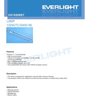
1. Product Overview
This document details the specifications for a high-luminosity white light-emitting diode (LED) encapsulated in a popular T-1 (3mm) round package. The device is engineered to deliver superior luminous output, making it suitable for applications demanding high brightness and clear visibility. The core technology utilizes an InGaN semiconductor chip which emits blue light. This blue emission is then converted to a broad-spectrum white light through a phosphor layer deposited within the LED's reflector cup. The resulting typical chromaticity coordinates are x=0.29, y=0.28 according to the CIE 1931 color space standard, indicating a neutral to cool white color temperature. The component is designed for reliability and includes features such as electrostatic discharge (ESD) protection up to 4KV (Human Body Model) and compliance with relevant environmental regulations.
1.1 Core Advantages and Target Market
The primary advantage of this LED is its high luminous intensity within a compact, industry-standard T-1 form factor. This combination of small size and high brightness offers design engineers significant flexibility. The device is supplied in bulk or on tape and reel for automated assembly processes, enhancing manufacturing efficiency. Its key applications are centered around areas requiring clear, bright indication or illumination. The target markets include consumer electronics, industrial control panels, automotive interior lighting, and general signage.
2. Technical Parameter Deep-Dive
A comprehensive understanding of the electrical and optical limits is crucial for reliable circuit design and long-term performance.
2.1 Absolute Maximum Ratings
These ratings define the stress limits beyond which permanent damage to the device may occur. Operation under or at these limits is not guaranteed and should be avoided for reliable performance.
- Continuous Forward Current (IF): 30 mA. This is the maximum DC current that can be applied continuously to the LED.
- Peak Forward Current (IFP): 100 mA. This higher current is permissible only under pulsed conditions, specified at a duty cycle of 1/10 and a frequency of 1 kHz.
- Reverse Voltage (VR): 5 V. Applying a reverse bias voltage exceeding this value can cause junction breakdown.
- Power Dissipation (Pd): 110 mW. This is the maximum power the package can dissipate as heat, calculated as Forward Voltage (VF) multiplied by Forward Current (IF).
- Operating & Storage Temperature: The device can function in ambient temperatures from -40°C to +85°C and can be stored in temperatures from -40°C to +100°C.
- Soldering Temperature: The leads can withstand a soldering temperature of 260°C for a maximum duration of 5 seconds, which is compatible with standard reflow and hand-soldering processes.
2.2 Electro-Optical Characteristics
These parameters are measured under standard test conditions (Ta=25°C) and define the typical performance of the LED.
- Forward Voltage (VF): Ranges from 2.8V (Min) to 4.0V (Max) at a test current of 20mA. The typical value falls within this range. A current-limiting resistor is essential in series with the LED to control the current based on the supply voltage and the specific VF of the LED.
- Luminous Intensity (IV): Has a minimum value of 1800 millicandelas (mcd) at 20mA. The intensity can reach up to 4500 mcd depending on the specific bin (see Section 3). This high intensity is a key feature.
- Viewing Angle (2θ1/2): The typical full viewing angle at half intensity is 25 degrees. This indicates a relatively focused beam pattern, which is ideal for directional indication.
- Reverse Current (IR): Is limited to a maximum of 50 µA when a 5V reverse bias is applied, indicating good junction integrity.
- Zener Diode Feature: The datasheet notes a Zener Reverse Voltage (VZ) of 5.2V typ. at 5mA and a Zener Reverse Current (IZ) rating of 100mA. This suggests some units may incorporate an integrated reverse-voltage protection Zener diode, but designers should confirm this feature's availability and specifications for their specific application.
3. Binning System Explanation
Due to manufacturing variances, LEDs are sorted into performance bins. Understanding these bins is critical for achieving consistent color and brightness in an application.
3.1 Luminous Intensity Binning
LEDs are categorized into four intensity bins (M, N, P, Q) based on their measured luminous output at 20mA. The tolerance for luminous intensity is ±10% within each bin.
- Bin M: 1800 mcd to 2250 mcd
- Bin N: 2250 mcd to 2850 mcd
- Bin P: 2850 mcd to 3600 mcd
- Bin Q: 3600 mcd to 4500 mcd
3.2 Forward Voltage Binning
LEDs are also binned according to their forward voltage drop at 20mA, with a measurement uncertainty of ±0.1V. This helps in designing consistent current drive circuits, especially when multiple LEDs are connected in parallel.
- Bin 0: 2.8V to 3.0V
- Bin 1: 3.0V to 3.5V
- Bin 2: 3.5V to 4.0V
3.3 Color Coordinate Binning (Chromaticity)
The white light color is defined by its coordinates on the CIE 1931 chromaticity diagram. The LEDs are grouped into eight color ranks (A1, A2, B1, B2, C1, C2, D1, D2), each with defined minimum and maximum boundaries for both the x and y coordinates. The typical coordinate is x=0.29, y=0.28, which would fall within the C1 or C2 bins. The measurement uncertainty for color coordinates is ±0.01. This binning ensures color consistency for applications where uniform white appearance is important.
4. Performance Curve Analysis
Graphical data provides insight into how the LED behaves under varying conditions.
4.1 Relative Intensity vs. Wavelength
The spectral power distribution curve shows the relative intensity of light emitted across different wavelengths. For a white LED using a blue chip + phosphor system, this curve typically shows a dominant peak in the blue region (around 450-460nm from the InGaN chip) and a broader peak or plateau in the yellow/green/red region (from the phosphor). The combined output is perceived as white light.
4.2 Forward Current vs. Forward Voltage (I-V Curve)
This curve is non-linear, characteristic of a diode. The voltage increases gradually with current initially and then more steeply. Operating the LED at the recommended 20mA ensures it is on the efficient, stable part of this curve.
4.3 Relative Intensity vs. Forward Current
Luminous output is directly proportional to forward current, but the relationship is not perfectly linear, especially at higher currents due to efficiency droop and thermal effects. Increasing current beyond the recommended maximum will not yield proportional increases in light and will generate excessive heat.
4.4 Chromaticity Coordinate vs. Forward Current
This graph illustrates how the color point (x, y coordinates) may shift slightly with changes in drive current. Typically, higher currents can cause a small blue shift due to increased chip temperature and changes in phosphor conversion efficiency.
4.5 Forward Current vs. Ambient Temperature
The LED's maximum permissible forward current decreases as the ambient temperature increases. This derating is necessary to prevent the junction temperature from exceeding its limit, which would accelerate lumen depreciation and reduce lifespan. Designers must consider the operating environment's temperature when setting the drive current.
5. Mechanical and Packaging Information
5.1 Package Dimensions
The LED conforms to the standard T-1 3mm round package dimensions. Key measurements include a typical body diameter of 3.0mm and a height of approximately 5.0mm from the bottom of the flange to the top of the lens. The leads have a diameter of 0.45mm and are spaced 2.54mm apart (standard 0.1-inch pitch). The lens is water-clear. All dimensional tolerances are ±0.25mm unless otherwise specified. The lead spacing is measured where the leads emerge from the package body. A maximum resin protrusion of 1.5mm under the flange is allowed.
5.2 Polarity Identification
The LED is a polarized component. The longer lead is typically the anode (positive), and the shorter lead is the cathode (negative). Additionally, the cathode side often has a flat spot on the plastic flange or a notch in the rim. Correct polarity must be observed during circuit assembly.
6. Soldering and Assembly Guidelines
Proper handling is essential to prevent damage and ensure reliability.
6.1 Lead Forming
- Bending must occur at a point at least 3mm from the base of the epoxy bulb to avoid stress on the internal wire bonds and die.
- Forming should always be done before soldering.
- Excessive stress on the package during bending must be avoided.
- Cutting of leads should be performed at room temperature.
- PCB holes must align precisely with the LED leads to avoid mounting stress.
6.2 Storage Conditions
LEDs are moisture-sensitive devices. After receipt, they should be stored at 30°C or less and 70% relative humidity (RH) or less. The recommended storage life under these conditions is 3 months. For longer storage (up to one year), the devices should be kept in a sealed, moisture-barrier bag with desiccant and in a nitrogen atmosphere if possible. Rapid temperature changes in humid environments should be avoided to prevent condensation.
6.3 Soldering Recommendations
A minimum distance of 3mm must be maintained between the solder joint and the epoxy bulb to prevent thermal damage.
- Hand Soldering: Use an iron with a tip temperature not exceeding 300°C (for a maximum 30W iron). Contact time should be 3 seconds or less per lead.
- Wave or Dip Soldering: Preheat temperature should not exceed 100°C for a maximum of 60 seconds. The solder bath temperature should not exceed 260°C, with a contact time of 5 seconds or less.
7. Packaging and Ordering Information
7.1 Packing Specification
The LEDs are packed in anti-static bags to protect against electrostatic discharge. The packing hierarchy is as follows:
- Inner Pack: A minimum of 200 to a maximum of 500 pieces are placed in one anti-static bag.
- Inner Carton: Five anti-static bags are packed into one inner carton.
- Master (Outside) Carton: Ten inner cartons are packed into one master shipping carton.
7.2 Label Information
Packaging labels include several codes: Customer's Production Number (CPN), Production Number (P/N), Packing Quantity (QTY), combined ranks for Luminous Intensity and Forward Voltage (CAT), Color Rank (HUE), Reference (REF), and Lot Number (LOT No.).
8. Application Suggestions
8.1 Typical Application Scenarios
- Message Panels & Signage: Ideal for backlighting or as individual status indicators in information displays due to high brightness.
- Optical Indicators: Perfect for power, status, or alert indicators in consumer electronics, industrial equipment, and automotive dashboards.
- Backlighting: Can be used for small-scale backlighting of switches, keypads, or LCD panels.
- Marker Lights: Suitable for decorative or positional lighting.
8.2 Design Considerations
- Current Limiting: Always use a series resistor or a constant-current driver to set the forward current. Calculate the resistor value using R = (Vsupply - VF) / IF.
- Thermal Management: While the power is low, ensure adequate ventilation if multiple LEDs are used in a confined space or if operating at high ambient temperatures.
- Reverse Voltage Protection: If the integrated Zener feature is not confirmed or sufficient, consider adding an external protection diode in parallel (cathode to anode) with the LED if the circuit is exposed to reverse voltage transients.
- Binning for Consistency: For applications requiring uniform brightness or color, specify the required intensity and color bins when ordering.
9. Technical Comparison and Differentiation
Compared to standard indicator LEDs, this device's primary differentiator is its very high luminous intensity (up to 4500 mcd) within the common T-1 package. Many standard white T-1 LEDs offer intensities in the range of 200-1000 mcd. This makes it a drop-in replacement for applications requiring a significant boost in brightness without changing the footprint or lens optics. The inclusion of ESD protection (4KV HBM) also enhances its robustness compared to basic LEDs without such protection, making it more suitable for environments with handling or static discharge concerns.
10. Frequently Asked Questions (Based on Technical Parameters)
10.1 What resistor do I need for a 5V supply?
Using the worst-case maximum forward voltage (VF = 4.0V) and a target current of 20mA, the calculation is: R = (5V - 4.0V) / 0.020A = 50 Ohms. The nearest standard value is 51 Ohms. The power dissipated in the resistor is P = I2R = (0.02)2 * 51 = 0.0204W, so a standard 1/4W resistor is sufficient. Always verify with the actual VF of your specific LED bin for optimal current.
10.2 Can I drive it at 30mA continuously?
Yes, 30mA is the absolute maximum continuous forward current rating. However, for maximum longevity and to account for potential temperature rises in the application, operating at or slightly below the typical 20mA is recommended. At 30mA, ensure the ambient temperature is not at the upper limit of 85°C.
10.3 How do I interpret the color bins (A1, B2, etc.)?
The letter (A, B, C, D) generally indicates a region on the CIE diagram, often correlating with correlated color temperature (CCT). 'A' bins are typically warmer white (more yellow/red), progressing to 'D' bins which are cooler white (more blue). The number (1, 2) further subdivides the region. For most general applications, specifying a range like B-C is sufficient. For critical color-matching applications, the exact bin should be specified and controlled.
11. Practical Design Case Study
Scenario: Designing a high-visibility status indicator panel for an outdoor telecommunications cabinet. The panel has 10 indicators that must be clearly visible in direct sunlight. Space is limited, requiring a small component. The T-1 package is selected for its size. This high-intensity LED (using Bin Q for maximum brightness) is chosen. A 12V supply is available in the cabinet. Design steps: 1) Calculate series resistor. Using VF (Bin 1 typical ~3.2V) and IF=20mA: R = (12V - 3.2V) / 0.02A = 440 Ohms (use 470 Ohms standard, resulting in IF ≈ 18.7mA). 2) Calculate resistor power: P = (0.0187)2 * 470 ≈ 0.164W (a 1/4W resistor is adequate but a 1/2W provides margin). 3) Layout: Ensure 3mm spacing from PCB hole to LED body for soldering. 4) Consider adding a transient voltage suppression diode on the 12V line if the environment is electrically noisy.
12. Operating Principle Introduction
This is a phosphor-converted white LED. The heart of the device is a semiconductor die made of Indium Gallium Nitride (InGaN). When a forward voltage is applied, electrons and holes recombine within the active region of the InGaN structure, emitting photons. The bandgap of the InGaN material is engineered to produce blue light with a wavelength around 450-460 nanometers. This blue light then strikes a layer of phosphor, which is a ceramic material doped with rare-earth elements (often yttrium aluminum garnet doped with cerium, or YAG:Ce). The phosphor absorbs a portion of the blue photons and re-emits light at longer, broader wavelengths across the yellow and red spectrum. The human eye perceives the mix of the remaining direct blue light and the phosphor-converted yellow/red light as white light. The specific ratios of blue to yellow/red determine the color temperature and chromaticity coordinates.
13. Technology Trends and Context
The development of efficient blue InGaN LEDs, for which the Nobel Prize in Physics was awarded in 2014, enabled the creation of practical white LEDs via phosphor conversion. The trend in the industry has been towards ever-higher efficiency (more lumens per watt), higher reliability, and better color rendering. While this datasheet describes a mid-power LED in a through-hole package, the broader market has seen a massive shift towards surface-mount device (SMD) packages (like 2835, 3030, 5050) for most general lighting and backlighting applications due to better thermal performance and suitability for automated assembly. However, through-hole LEDs like this T-1 package remain vital for prototyping, educational use, repair markets, and applications where manual assembly or robustness of the leaded connection is preferred. The integration of features like ESD protection and more precise binning, as seen in this datasheet, represents an evolution of these mature package types to meet modern reliability and performance demands.
LED Specification Terminology
Complete explanation of LED technical terms
Photoelectric Performance
| Term | Unit/Representation | Simple Explanation | Why Important |
|---|---|---|---|
| Luminous Efficacy | lm/W (lumens per watt) | Light output per watt of electricity, higher means more energy efficient. | Directly determines energy efficiency grade and electricity cost. |
| Luminous Flux | lm (lumens) | Total light emitted by source, commonly called "brightness". | Determines if the light is bright enough. |
| Viewing Angle | ° (degrees), e.g., 120° | Angle where light intensity drops to half, determines beam width. | Affects illumination range and uniformity. |
| CCT (Color Temperature) | K (Kelvin), e.g., 2700K/6500K | Warmth/coolness of light, lower values yellowish/warm, higher whitish/cool. | Determines lighting atmosphere and suitable scenarios. |
| CRI / Ra | Unitless, 0–100 | Ability to render object colors accurately, Ra≥80 is good. | Affects color authenticity, used in high-demand places like malls, museums. |
| SDCM | MacAdam ellipse steps, e.g., "5-step" | Color consistency metric, smaller steps mean more consistent color. | Ensures uniform color across same batch of LEDs. |
| Dominant Wavelength | nm (nanometers), e.g., 620nm (red) | Wavelength corresponding to color of colored LEDs. | Determines hue of red, yellow, green monochrome LEDs. |
| Spectral Distribution | Wavelength vs intensity curve | Shows intensity distribution across wavelengths. | Affects color rendering and quality. |
Electrical Parameters
| Term | Symbol | Simple Explanation | Design Considerations |
|---|---|---|---|
| Forward Voltage | Vf | Minimum voltage to turn on LED, like "starting threshold". | Driver voltage must be ≥Vf, voltages add up for series LEDs. |
| Forward Current | If | Current value for normal LED operation. | Usually constant current drive, current determines brightness & lifespan. |
| Max Pulse Current | Ifp | Peak current tolerable for short periods, used for dimming or flashing. | Pulse width & duty cycle must be strictly controlled to avoid damage. |
| Reverse Voltage | Vr | Max reverse voltage LED can withstand, beyond may cause breakdown. | Circuit must prevent reverse connection or voltage spikes. |
| Thermal Resistance | Rth (°C/W) | Resistance to heat transfer from chip to solder, lower is better. | High thermal resistance requires stronger heat dissipation. |
| ESD Immunity | V (HBM), e.g., 1000V | Ability to withstand electrostatic discharge, higher means less vulnerable. | Anti-static measures needed in production, especially for sensitive LEDs. |
Thermal Management & Reliability
| Term | Key Metric | Simple Explanation | Impact |
|---|---|---|---|
| Junction Temperature | Tj (°C) | Actual operating temperature inside LED chip. | Every 10°C reduction may double lifespan; too high causes light decay, color shift. |
| Lumen Depreciation | L70 / L80 (hours) | Time for brightness to drop to 70% or 80% of initial. | Directly defines LED "service life". |
| Lumen Maintenance | % (e.g., 70%) | Percentage of brightness retained after time. | Indicates brightness retention over long-term use. |
| Color Shift | Δu′v′ or MacAdam ellipse | Degree of color change during use. | Affects color consistency in lighting scenes. |
| Thermal Aging | Material degradation | Deterioration due to long-term high temperature. | May cause brightness drop, color change, or open-circuit failure. |
Packaging & Materials
| Term | Common Types | Simple Explanation | Features & Applications |
|---|---|---|---|
| Package Type | EMC, PPA, Ceramic | Housing material protecting chip, providing optical/thermal interface. | EMC: good heat resistance, low cost; Ceramic: better heat dissipation, longer life. |
| Chip Structure | Front, Flip Chip | Chip electrode arrangement. | Flip chip: better heat dissipation, higher efficacy, for high-power. |
| Phosphor Coating | YAG, Silicate, Nitride | Covers blue chip, converts some to yellow/red, mixes to white. | Different phosphors affect efficacy, CCT, and CRI. |
| Lens/Optics | Flat, Microlens, TIR | Optical structure on surface controlling light distribution. | Determines viewing angle and light distribution curve. |
Quality Control & Binning
| Term | Binning Content | Simple Explanation | Purpose |
|---|---|---|---|
| Luminous Flux Bin | Code e.g., 2G, 2H | Grouped by brightness, each group has min/max lumen values. | Ensures uniform brightness in same batch. |
| Voltage Bin | Code e.g., 6W, 6X | Grouped by forward voltage range. | Facilitates driver matching, improves system efficiency. |
| Color Bin | 5-step MacAdam ellipse | Grouped by color coordinates, ensuring tight range. | Guarantees color consistency, avoids uneven color within fixture. |
| CCT Bin | 2700K, 3000K etc. | Grouped by CCT, each has corresponding coordinate range. | Meets different scene CCT requirements. |
Testing & Certification
| Term | Standard/Test | Simple Explanation | Significance |
|---|---|---|---|
| LM-80 | Lumen maintenance test | Long-term lighting at constant temperature, recording brightness decay. | Used to estimate LED life (with TM-21). |
| TM-21 | Life estimation standard | Estimates life under actual conditions based on LM-80 data. | Provides scientific life prediction. |
| IESNA | Illuminating Engineering Society | Covers optical, electrical, thermal test methods. | Industry-recognized test basis. |
| RoHS / REACH | Environmental certification | Ensures no harmful substances (lead, mercury). | Market access requirement internationally. |
| ENERGY STAR / DLC | Energy efficiency certification | Energy efficiency and performance certification for lighting. | Used in government procurement, subsidy programs, enhances competitiveness. |