Table of Contents
- 1. Product Overview
- 2. In-Depth Technical Parameter Analysis
- 2.1 Absolute Maximum Ratings
- 2.2 Electrical Characteristics
- 2.3 Switching Characteristics
- 3. Pin Configuration and Schematic
- 4. Truth Table and Logic Function
- 5. Mechanical and Packaging Information
- 6. Soldering and Assembly Guidelines
- 7. Application Suggestions
- 7.1 Typical Application Scenarios
- 7.2 Design Considerations
- 8. Technical Comparison and Differentiation
- 9. Frequently Asked Questions (Based on Technical Parameters)
- 10. Practical Design and Usage Case
- 11. Operating Principle
- 12. Industry Trends and Context
1. Product Overview
The EL260L is a high-speed logic gate photocoupler designed for digital signal isolation. It integrates an infrared emitting diode optically coupled to a high-speed integrated photo-detector with a strobable logic gate output. Packaged in an 8-pin Dual In-line Package (DIP), it is engineered to provide reliable electrical isolation and signal integrity in demanding applications.
Core Advantages: The device's primary strengths include its high-speed data transmission capability of up to 10 Mbit/s, robust common-mode transient immunity (CMTI) of 10 kV/μs minimum, and dual supply voltage compatibility (3.3V and 5V). It guarantees performance across a wide operating temperature range from -40°C to +85°C. The logic gate output can drive up to 10 standard loads (Fan-out 10).
Target Market: This component is targeted at applications requiring high-speed digital isolation, ground loop elimination, and noise immunity in industrial automation, power supply systems, computer peripherals, and communication interfaces.
2. In-Depth Technical Parameter Analysis
2.1 Absolute Maximum Ratings
The Absolute Maximum Ratings define the stress limits beyond which permanent damage to the device may occur. Key parameters include a maximum forward current (IF) of 50 mA for the input LED, a reverse voltage (VR) of 5 V, and supply/output voltages (VCC, VO) of 7.0 V. The total power dissipation for the input side is 45 mW, while the output side can handle 85 mW. The isolation voltage (VISO) between input and output is rated at 5000 Vrms for one minute. Operating and storage temperature ranges are -40°C to +85°C and -55°C to +125°C, respectively. The device can withstand a soldering temperature of 260°C for 10 seconds.
2.2 Electrical Characteristics
These specifications detail the device's performance under normal operating conditions (TA = -40°C to 85°C).
Input Characteristics: The forward voltage (VF) typically measures 1.4V at IF=10mA, with a maximum of 1.8V. The input capacitance (CIN) is typically 60 pF.
Output Characteristics: Supply current varies with state: ICCH (high level) is typically 7 mA (max 10 mA), and ICCL (low level) is typically 9 mA (max 13 mA) at VCC=3.3V. The enable input has an internal pull-up resistor, requiring no external component. The low-level enable voltage (VEL) is guaranteed to be below 0.8V.
Transfer Characteristics: Critical for logic operation, the low-level output voltage (VOL) is typically 0.35V (max 0.6V) when sinking 13 mA. The input threshold current (IFT) to trigger a logic low output is typically 2.5 mA (max 5 mA).
2.3 Switching Characteristics
Measured at VCC=3.3V, IF=7.5mA, with a load of RL=350Ω and CL=15pF.
Propagation Delays: The propagation delay time to output low (tPHL) is typically 40 ns (max 75 ns), and to output high (tPLH) is typically 45 ns (max 75 ns). Pulse width distortion, the absolute difference between tPHL and tPLH, is typically 5 ns (max 35 ns), crucial for timing-sensitive applications.
Transition Times: Output rise time (tr) is typically 40 ns, while fall time (tf) is typically 10 ns, indicating faster turn-off.
Enable Times: The enable propagation delay to output low (tEHL) is typically 10 ns, and to output high (tELH) is typically 25 ns.
Common-Mode Transient Immunity (CMTI): A key isolation metric. The device guarantees a minimum of 10,000 V/μs for both logic high (CMH) and logic low (CML) states, ensuring reliable operation in noisy environments with fast voltage transients across the isolation barrier.
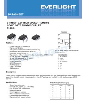
3. Pin Configuration and Schematic
The 8-pin DIP configuration is as follows: Pin 1 (NC), Pin 2 (Anode), Pin 3 (Cathode), Pin 4 (NC), Pin 5 (GND), Pin 6 (VOUT), Pin 7 (VE - Enable), Pin 8 (VCC). A critical design requirement is the placement of a 0.1μF (or larger) bypass capacitor with good high-frequency characteristics between pins 8 (VCC) and 5 (GND), located as close as possible to the package to ensure stable operation and minimize noise.
4. Truth Table and Logic Function
The device functions as a strobable logic gate. The truth table (using positive logic) defines its operation:
- Input (IF) High, Enable (VE) High: Output (VO) = Low
- Input Low, Enable High: Output = High
- Input High, Enable Low: Output = High
- Input Low, Enable Low: Output = High
- Input High, Enable NC (No Connection): Output = Low
- Input Low, Enable NC: Output = High
The enable pin provides a third-state control, allowing the output to be forced high regardless of the input signal when the enable is low.
5. Mechanical and Packaging Information
The device is offered in a standard 8-pin DIP package. The datasheet indicates availability in both wide-lead spacing and Surface-Mount Device (SMD) options, though the primary focus here is the through-hole DIP variant. Detailed dimensional drawings would typically be included in a full datasheet to guide PCB layout and footprint design.
6. Soldering and Assembly Guidelines
The Absolute Maximum Ratings specify a soldering temperature (TSOL) of 260°C for 10 seconds. This is a critical parameter for wave or reflow soldering processes. Standard IPC guidelines for through-hole component soldering should be followed. Proper ESD handling procedures are recommended during assembly due to the sensitive semiconductor components inside.
7. Application Suggestions
7.1 Typical Application Scenarios
- Ground Loop Elimination & Logic Level Translation: Isolating digital signals between circuits with different ground potentials, such as translating signals between LSTTL and TTL/CMOS logic families.
- Data Transmission & Multiplexing: High-speed serial data isolation in communication lines and data bus isolation.
- Switching Power Supplies: Providing feedback isolation in flyback or other isolated converter topologies.
- Pulse Transformer Replacement: Offering a solid-state, potentially more compact and reliable alternative to traditional pulse transformers for signal isolation.
- Computer Peripheral & Industrial Interface: Isolating digital I/O lines in noisy industrial environments or for interfacing with motors and actuators.
7.2 Design Considerations
- Bypass Capacitor: The 0.1μF capacitor across VCC and GND is mandatory for stable high-speed operation and must be placed close to the pins.
- Current Limiting Resistor: An external resistor is required in series with the input LED (Anode) to set the forward current (IF) according to the application needs (e.g., 7.5mA for specified switching times).
- Load Resistor: The output characteristics are specified with a 350Ω pull-up resistor to VCC. This value must be used or adjusted carefully based on the required output current and speed.
- Enable Pin: The internal pull-up on the enable pin simplifies design. Driving it low forces the output high; leaving it unconnected (NC) defaults to a high state, allowing normal operation controlled solely by the input.
- PCB Layout: Maintain good isolation clearance and creepage distances on the PCB between the input and output sides as per safety standards, even though the component itself provides the primary isolation barrier.
8. Technical Comparison and Differentiation
The EL260L differentiates itself in the photocoupler market through its combination of high speed (10 Mbit/s) and exceptionally high CMTI (10 kV/μs). Many standard photocouplers operate at lower speeds (e.g., 1 Mbit/s) or have lower CMTI ratings. The dual 3.3V/5V supply compatibility offers design flexibility in modern mixed-voltage systems. The integrated logic gate with enable function and guaranteed performance over a wide temperature range makes it a robust choice for industrial applications compared to basic transistor-output optocouplers.
9. Frequently Asked Questions (Based on Technical Parameters)
Q: What is the purpose of the enable (VE) pin?
A: The enable pin provides a third-state control. When driven low, it overrides the input signal and forces the output to a logic high state. This can be used for bus contention management or to disable the output.
Q: Why is the 0.1μF bypass capacitor so critical?
A: At high switching speeds (10 Mbit/s), sudden current demands can cause voltage spikes on the supply rail. The local bypass capacitor provides a immediate charge reservoir, stabilizing VCC and preventing malfunctions or noise generation.
Q: How do I select the value for the input current limiting resistor?
A: Use Ohm's Law: RLIMIT = (Supply Voltage - VF) / IF. For example, with a 5V supply, VF~1.4V, and desired IF=10mA: R = (5 - 1.4) / 0.01 = 360Ω. Choose a standard value like 360Ω or 390Ω. For optimal speed, use IF=7.5mA as per the switching specs.
Q: Can I use this with a 5V supply for the output side?
A: Yes, the datasheet specifies dual supply voltage compatibility (3.3V and 5V). The electrical characteristics tables often list conditions at VCC=3.3V, but the device is designed to operate with 5V as well. Always check all parameters at your intended supply voltage.
10. Practical Design and Usage Case
Scenario: Isolated RS-485/RS-422 Transceiver Interface. In an industrial sensor node, a microcontroller communicates with an RS-485 transceiver over UART. To protect the sensitive microcontroller from ground shifts and high-voltage transients on the long RS-485 bus, the EL260L can be used to isolate the UART TX and RX lines. The microcontroller side (input) operates at 3.3V, while the transceiver side (output) can operate at 5V. The high 10 Mbit/s speed easily handles standard serial baud rates (e.g., 115200 baud, 1 Mbaud). The 10 kV/μs CMTI ensures the isolation remains effective even during severe electrical noise events on the bus. The enable pin could be tied to a microcontroller GPIO to disable the communication path if needed.
11. Operating Principle
The EL260L operates on the principle of optical coupling. An electrical current applied to the input side (pins 2 & 3) causes an infrared Light Emitting Diode (LED) to emit light. This light traverses a transparent isolation barrier within the package. On the output side, a high-speed integrated photodetector converts the received light back into an electrical current. This current is processed by an internal amplifier and logic gate circuit to produce a clean, buffered digital output signal (on pin 6) that mirrors the state of the input but is electrically isolated from it. The isolation barrier, typically made of mold compound or similar material, provides the high voltage isolation (5000 Vrms) between the two sides.
12. Industry Trends and Context
The demand for high-speed digital isolators is driven by several trends: the proliferation of industrial IoT and automation requiring robust communication in noisy environments; the adoption of higher switching frequencies in power electronics necessitating faster feedback isolation; and the move towards higher system-level integration and reliability. Components like the EL260L represent a mature and cost-effective technology for galvanic isolation. The industry also sees growth in alternative isolation technologies like capacitive and magnetic (giant magnetoresistance) isolators, which can offer even higher speeds, lower power consumption, and greater integration density. However, photocouplers remain highly popular due to their simplicity, proven reliability, high CMTI, and ease of use in a wide range of applications. The focus for advanced photocouplers continues to be on increasing speed, improving power efficiency, reducing package size, and enhancing reliability metrics like long-term insulation resistance.
LED Specification Terminology
Complete explanation of LED technical terms
Photoelectric Performance
| Term | Unit/Representation | Simple Explanation | Why Important |
|---|---|---|---|
| Luminous Efficacy | lm/W (lumens per watt) | Light output per watt of electricity, higher means more energy efficient. | Directly determines energy efficiency grade and electricity cost. |
| Luminous Flux | lm (lumens) | Total light emitted by source, commonly called "brightness". | Determines if the light is bright enough. |
| Viewing Angle | ° (degrees), e.g., 120° | Angle where light intensity drops to half, determines beam width. | Affects illumination range and uniformity. |
| CCT (Color Temperature) | K (Kelvin), e.g., 2700K/6500K | Warmth/coolness of light, lower values yellowish/warm, higher whitish/cool. | Determines lighting atmosphere and suitable scenarios. |
| CRI / Ra | Unitless, 0–100 | Ability to render object colors accurately, Ra≥80 is good. | Affects color authenticity, used in high-demand places like malls, museums. |
| SDCM | MacAdam ellipse steps, e.g., "5-step" | Color consistency metric, smaller steps mean more consistent color. | Ensures uniform color across same batch of LEDs. |
| Dominant Wavelength | nm (nanometers), e.g., 620nm (red) | Wavelength corresponding to color of colored LEDs. | Determines hue of red, yellow, green monochrome LEDs. |
| Spectral Distribution | Wavelength vs intensity curve | Shows intensity distribution across wavelengths. | Affects color rendering and quality. |
Electrical Parameters
| Term | Symbol | Simple Explanation | Design Considerations |
|---|---|---|---|
| Forward Voltage | Vf | Minimum voltage to turn on LED, like "starting threshold". | Driver voltage must be ≥Vf, voltages add up for series LEDs. |
| Forward Current | If | Current value for normal LED operation. | Usually constant current drive, current determines brightness & lifespan. |
| Max Pulse Current | Ifp | Peak current tolerable for short periods, used for dimming or flashing. | Pulse width & duty cycle must be strictly controlled to avoid damage. |
| Reverse Voltage | Vr | Max reverse voltage LED can withstand, beyond may cause breakdown. | Circuit must prevent reverse connection or voltage spikes. |
| Thermal Resistance | Rth (°C/W) | Resistance to heat transfer from chip to solder, lower is better. | High thermal resistance requires stronger heat dissipation. |
| ESD Immunity | V (HBM), e.g., 1000V | Ability to withstand electrostatic discharge, higher means less vulnerable. | Anti-static measures needed in production, especially for sensitive LEDs. |
Thermal Management & Reliability
| Term | Key Metric | Simple Explanation | Impact |
|---|---|---|---|
| Junction Temperature | Tj (°C) | Actual operating temperature inside LED chip. | Every 10°C reduction may double lifespan; too high causes light decay, color shift. |
| Lumen Depreciation | L70 / L80 (hours) | Time for brightness to drop to 70% or 80% of initial. | Directly defines LED "service life". |
| Lumen Maintenance | % (e.g., 70%) | Percentage of brightness retained after time. | Indicates brightness retention over long-term use. |
| Color Shift | Δu′v′ or MacAdam ellipse | Degree of color change during use. | Affects color consistency in lighting scenes. |
| Thermal Aging | Material degradation | Deterioration due to long-term high temperature. | May cause brightness drop, color change, or open-circuit failure. |
Packaging & Materials
| Term | Common Types | Simple Explanation | Features & Applications |
|---|---|---|---|
| Package Type | EMC, PPA, Ceramic | Housing material protecting chip, providing optical/thermal interface. | EMC: good heat resistance, low cost; Ceramic: better heat dissipation, longer life. |
| Chip Structure | Front, Flip Chip | Chip electrode arrangement. | Flip chip: better heat dissipation, higher efficacy, for high-power. |
| Phosphor Coating | YAG, Silicate, Nitride | Covers blue chip, converts some to yellow/red, mixes to white. | Different phosphors affect efficacy, CCT, and CRI. |
| Lens/Optics | Flat, Microlens, TIR | Optical structure on surface controlling light distribution. | Determines viewing angle and light distribution curve. |
Quality Control & Binning
| Term | Binning Content | Simple Explanation | Purpose |
|---|---|---|---|
| Luminous Flux Bin | Code e.g., 2G, 2H | Grouped by brightness, each group has min/max lumen values. | Ensures uniform brightness in same batch. |
| Voltage Bin | Code e.g., 6W, 6X | Grouped by forward voltage range. | Facilitates driver matching, improves system efficiency. |
| Color Bin | 5-step MacAdam ellipse | Grouped by color coordinates, ensuring tight range. | Guarantees color consistency, avoids uneven color within fixture. |
| CCT Bin | 2700K, 3000K etc. | Grouped by CCT, each has corresponding coordinate range. | Meets different scene CCT requirements. |
Testing & Certification
| Term | Standard/Test | Simple Explanation | Significance |
|---|---|---|---|
| LM-80 | Lumen maintenance test | Long-term lighting at constant temperature, recording brightness decay. | Used to estimate LED life (with TM-21). |
| TM-21 | Life estimation standard | Estimates life under actual conditions based on LM-80 data. | Provides scientific life prediction. |
| IESNA | Illuminating Engineering Society | Covers optical, electrical, thermal test methods. | Industry-recognized test basis. |
| RoHS / REACH | Environmental certification | Ensures no harmful substances (lead, mercury). | Market access requirement internationally. |
| ENERGY STAR / DLC | Energy efficiency certification | Energy efficiency and performance certification for lighting. | Used in government procurement, subsidy programs, enhances competitiveness. |