Table of Contents
- 1. Product Overview
- 1.1 Core Advantages and Product Positioning
- 1.2 Key Features Summary
- 2. Technical Parameters: In-Depth Objective Interpretation
- 2.1 Absolute Maximum Ratings
- 2.2 Electro-Optical Characteristics
- 3. Binning System Explanation
- 3.1 Luminous Intensity Binning
- 3.2 Dominant Wavelength Binning
- 3.3 Forward Voltage Binning
- 4. Performance Curve Analysis
- 4.1 Inferred Current-Voltage (I-V) Relationship
- 4.2 Luminous Intensity vs. Current (L-I)
- 4.3 Temperature Dependence
- 5. Mechanical and Package Information
- 5.1 Package Dimensions
- 6. Soldering and Assembly Guidelines
- 6.1 Current Limiting and Protection
- 6.2 Storage and Moisture Sensitivity
- 6.3 Reflow Soldering Profile
- 6.4 Hand Soldering and Rework
- 7. Packaging and Ordering Information
- 7.1 Reel and Tape Specifications
- 7.2 Label Information
- 8. Application Suggestions and Design Considerations
- 8.1 Typical Application Scenarios
- 8.2 Critical Design Considerations
- 9. Technical Comparison and Differentiation
- 10. Frequently Asked Questions (Based on Technical Parameters)
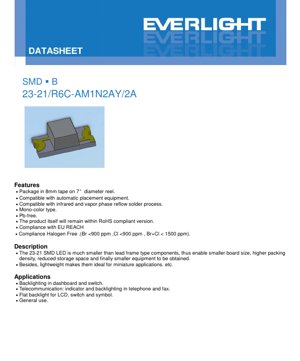
1. Product Overview
The 23-21 SMD LED is a compact, surface-mount light-emitting diode designed for modern electronic applications requiring reliable indicator lighting or backlighting in constrained spaces. This component represents a significant advancement over traditional lead-frame type LEDs, offering substantial benefits in terms of board real estate, assembly efficiency, and final product size.
1.1 Core Advantages and Product Positioning
The primary advantage of the 23-21 SMD LED lies in its miniature footprint. With dimensions of approximately 2.3mm x 2.1mm, it enables significant reductions in printed circuit board (PCB) size. This directly translates to higher component packing density, allowing for more complex functionality within a smaller overall device profile. The reduced storage space requirements for both the components themselves and the finished assemblies offer logistical and cost benefits. Furthermore, the lightweight nature of the SMD package makes it an ideal candidate for portable and miniature applications where weight is a critical factor, such as in wearable technology, compact consumer electronics, and miniaturized control panels.
The product is positioned as a general-purpose indicator and backlight solution. It is not designed for high-power illumination but rather for status indication, symbolic backlighting, and low-level ambient lighting where consistent color and reliable performance are paramount.
1.2 Key Features Summary
- Packaging: Supplied in 8mm tape on 7-inch diameter reels, compatible with standard automated pick-and-place assembly equipment.
- Process Compatibility: Fully compatible with mainstream infrared (IR) and vapor phase reflow soldering processes.
- Type: Mono-color type, emitting a brilliant red light.
- Environmental Compliance: The product is Pb-free (lead-free), compliant with the RoHS (Restriction of Hazardous Substances) directive, compliant with EU REACH regulations, and meets halogen-free standards (Bromine <900 ppm, Chlorine <900 ppm, Br+Cl < 1500 ppm).
2. Technical Parameters: In-Depth Objective Interpretation
This section provides a detailed, objective analysis of the electrical, optical, and thermal parameters specified in the datasheet. Understanding these limits is crucial for reliable circuit design.
2.1 Absolute Maximum Ratings
The Absolute Maximum Ratings define the stress limits beyond which permanent damage to the device may occur. These are not operating conditions.
- Reverse Voltage (VR): 5V. Applying a reverse bias voltage exceeding this value can cause junction breakdown.
- Continuous Forward Current (IF): 25mA. This is the maximum DC current that can be passed through the LED continuously at an ambient temperature (Ta) of 25°C.
- Peak Forward Current (IFP): 60mA. This higher current is permissible only under pulsed conditions, specifically at a duty cycle of 1/10 and a frequency of 1kHz. It is useful for brief, high-intensity flashes but must not be used for DC operation.
- Power Dissipation (Pd): 60mW. This is the maximum amount of power the device can dissipate as heat. Exceeding this limit, typically by driving with too high a current or at too high an ambient temperature, will raise the junction temperature and degrade performance or cause failure.
- Electrostatic Discharge (ESD): Human Body Model (HBM) 2000V. This rating indicates a moderate level of ESD robustness. Standard ESD handling precautions (use of grounded workstations, wrist straps) are still required during assembly and handling.
- Operating Temperature (Topr): -40°C to +85°C. The LED is designed to function within this ambient temperature range.
- Storage Temperature (Tstg): -40°C to +90°C.
- Soldering Temperature: The device can withstand reflow soldering with a peak temperature of 260°C for up to 10 seconds, or hand soldering at 350°C for up to 3 seconds per terminal.
2.2 Electro-Optical Characteristics
These parameters are measured at a standard test condition of Ta=25°C and a forward current (IF) of 5mA, unless otherwise specified. They define the typical performance of the device.
- Luminous Intensity (Iv): Ranges from a minimum of 18.0 mcd to a maximum of 45.0 mcd. The actual value for a specific unit depends on its bin code (see Section 3). A typical value is not stated, implying significant variation across the production spread.
- Viewing Angle (2θ1/2): 130 degrees. This is the full angle at which the luminous intensity drops to half of its peak value. A 130° angle indicates a relatively wide viewing pattern, suitable for indicators that need to be seen from various angles.
- Peak Wavelength (λp): 632 nm (typical). This is the wavelength at which the spectral power output is maximum.
- Dominant Wavelength (λd): Ranges from 617.5 nm to 633.5 nm. This wavelength corresponds to the perceived color of the light and is more relevant for colorimetric applications than peak wavelength. The binning system categorizes devices based on this parameter.
- Spectral Bandwidth (Δλ): 20 nm (typical). This is the width of the emitted spectrum at half its maximum power. A value of 20nm is characteristic of AlGaInP-based red LEDs, indicating a relatively pure, saturated red color.
- Forward Voltage (VF): Ranges from 1.55V to 2.15V at IF=5mA. This parameter is also binned (see Section 3). The low forward voltage is a key advantage for low-voltage battery-operated circuits.
- Reverse Current (IR): Maximum of 10 µA at VR=5V. This specifies the maximum leakage current when the device is reverse-biased.
Note on Tolerances: The datasheet specifies separate tolerances for key parameters: Luminous Intensity (±11%), Dominant Wavelength (±1nm), and Forward Voltage (±0.1V). These tolerances apply on top of the bin ranges and must be considered in the tightest tolerance analysis.
3. Binning System Explanation
To ensure consistency in mass production, LEDs are sorted into performance bins. This allows designers to select parts that meet specific minimum criteria for their application.
3.1 Luminous Intensity Binning
Devices are categorized into four bins (M1, M2, N1, N2) based on their measured luminous intensity at IF=5mA.
- M1: 18.0 – 22.5 mcd
- M2: 22.5 – 28.5 mcd
- N1: 28.5 – 36.0 mcd
- N2: 36.0 – 45.0 mcd
Selection of a higher bin (e.g., N2) guarantees a brighter LED but may come at a higher cost. For applications where absolute brightness is not critical but consistency across multiple indicators is, specifying a single bin is essential.
3.2 Dominant Wavelength Binning
Color consistency is managed through four wavelength bins (E4, E5, E6, E7). This is crucial for applications where multiple LEDs are used together and must appear identical in color.
- E4: 617.5 – 621.5 nm (more orange-red)
- E5: 621.5 – 625.5 nm
- E6: 625.5 – 629.5 nm
- E7: 629.5 – 633.5 nm (more pure red)
3.3 Forward Voltage Binning
Three voltage bins (00, 0, 1) help in designing efficient current-limiting circuits, especially in parallel LED arrays where voltage matching can improve current sharing.
- 00: 1.55 – 1.75 V
- 0: 1.75 – 1.95 V
- 1: 1.95 – 2.15 V
4. Performance Curve Analysis
While the datasheet references "Typical Electro-Optical Characteristics Curves," the specific graphs are not provided in the text. Based on standard LED behavior and the given parameters, we can infer the likely relationships.
4.1 Inferred Current-Voltage (I-V) Relationship
The forward voltage (VF) is specified at 5mA. For a typical AlGaInP red LED, the I-V curve is exponential. Operating the LED at a current lower than 5mA will result in a proportionally lower VF (e.g., ~1.8-2.0V at 2mA). Driving it at the maximum continuous current of 25mA will cause VF to increase, likely to a value near the upper limit of its bin range or slightly above due to resistive heating in the semiconductor and contacts. A series resistor must always be used to limit the current, as the LED's dynamic resistance is very low and a small increase in voltage causes a large increase in current, risking thermal runaway.
4.2 Luminous Intensity vs. Current (L-I)
Luminous intensity is approximately proportional to forward current in the lower to mid-current range (up to ~20mA for such devices). The rated luminous intensity is at 5mA. Operating at 20mA would typically yield an intensity roughly 3.5 to 4 times higher, but this must be verified against the maximum power dissipation limit (60mW). At 20mA and a VF of 2.0V, power dissipation is 40mW, which is within the limit at 25°C. However, efficacy (light output per electrical watt) often decreases at higher currents due to increased heat.
4.3 Temperature Dependence
Key parameters are temperature-sensitive:
- Forward Voltage (VF): Decreases with increasing temperature (negative temperature coefficient, typically -2mV/°C for red LEDs). This can slightly increase current if driven by a constant voltage source with a series resistor.
- Luminous Intensity (Iv): Decreases with increasing junction temperature. The derating can be significant, often around 0.5-1% per °C rise above 25°C. Adequate thermal management on the PCB is necessary to maintain consistent brightness, especially in high ambient temperatures or when driven at higher currents.
- Dominant Wavelength (λd): Shifts slightly with temperature, typically at a rate of about 0.1 nm/°C for AlGaInP LEDs.
5. Mechanical and Package Information
5.1 Package Dimensions
The datasheet includes a detailed dimensioned drawing of the 23-21 SMD package. Key features include:
- The overall length is 2.3 mm and width is 2.1 mm (hence the 23-21 designation).
- The package has two anode/cathode terminals on the bottom side for surface mounting.
- A polarity indicator (likely a notch or a green marking on the top or bottom) is present to distinguish the cathode. Correct orientation is critical during assembly.
- The recommended land pattern (footprint) for PCB design is derived from these dimensions, typically including solder pads slightly larger than the device terminals to ensure a reliable solder fillet.
- All unspecified tolerances are ±0.1mm.
6. Soldering and Assembly Guidelines
Adherence to these guidelines is critical for yield and long-term reliability.
6.1 Current Limiting and Protection
Mandatory: An external current-limiting resistor must be used in series with the LED. The LED is a current-driven device. Without a resistor, even a small variation in the supply voltage (e.g., battery voltage drop) can cause a large, potentially destructive, increase in forward current.
6.2 Storage and Moisture Sensitivity
The LEDs are packaged in a moisture-resistant barrier bag with desiccant.
- Before Opening: Store at ≤30°C and ≤90% Relative Humidity (RH).
- After Opening: The "floor life" (time components can be exposed to ambient factory air) is 1 year at ≤30°C and ≤60% RH.
- Rebaking: If the desiccant indicates saturation (color change) or the floor life is exceeded, a rebake is required: 60°C ±5°C for 24 hours before use in a reflow process.
6.3 Reflow Soldering Profile
A lead-free (Pb-free) reflow profile is specified:
- Pre-heating: 150-200°C for 60-120 seconds.
- Time Above Liquidus (TAL): 60-150 seconds above 217°C.
- Peak Temperature: 260°C maximum, held for a maximum of 10 seconds.
- Heating Rate: Maximum 6°C/second.
- Time Above 255°C: Maximum 30 seconds.
- Cooling Rate: Maximum 3°C/second.
Important Restrictions: Reflow soldering should not be performed more than two times. Avoid mechanical stress on the package during heating and do not warp the PCB after soldering.
6.4 Hand Soldering and Rework
Hand soldering is permitted but requires extreme care to avoid thermal damage.
- Use a soldering iron with a tip temperature ≤350°C.
- Limit contact time to ≤3 seconds per terminal.
- Use a low-power iron (≤25W capacity).
- Allow a cooling interval of ≥2 seconds between soldering each terminal.
- Repair/Rework: Not recommended after the LED is soldered. If unavoidable, use a dual-head soldering iron to simultaneously heat both terminals for removal, minimizing stress on the solder joints and the LED's internal connections. Always verify post-rework functionality.
7. Packaging and Ordering Information
7.1 Reel and Tape Specifications
The product is supplied in industry-standard packaging for automated assembly:
- Carrier Tape Width: 8 mm.
- Reel Diameter: 7 inches.
- Quantity per Reel: 2000 pieces.
7.2 Label Information
The reel label contains critical information for traceability and correct application:
- CPN: Customer's Part Number (as assigned by the buyer).
- P/N: Manufacturer's Part Number (23-21/R6C-AM1N2AY/2A).
- QTY: Packing Quantity (2000).
- CAT: Luminous Intensity Rank (e.g., M1, N2).
- HUE: Chromaticity Coordinates & Dominant Wavelength Rank (e.g., E5, E6).
- REF: Forward Voltage Rank (e.g., 00, 1).
- LOT No: Manufacturing Lot Number for traceability.
8. Application Suggestions and Design Considerations
8.1 Typical Application Scenarios
- Automotive Interior: Backlighting for dashboard instruments, switches, and control panels.
- Telecommunications Equipment: Status indicators and keypad backlighting in telephones, fax machines, and networking hardware.
- Consumer Electronics: Flat backlighting for small LCD displays, backlighting for membrane switches and symbols on remote controls, appliances, and audio equipment.
- General Indication: Power status, mode indication, and alert signals in a wide variety of electronic devices.
8.2 Critical Design Considerations
- Current Drive Circuit: Always use a series resistor. Calculate the resistor value using R = (Vsupply - VF) / IF. Use the maximum VF from the bin (e.g., 2.15V) to ensure the current does not exceed the desired level even with the highest-voltage LED.
- Thermal Management: Although low power, consider the effect of ambient temperature and adjacent heat-generating components. For consistent brightness, avoid operating at the absolute maximum current (25mA) in high-temperature environments (>70°C).
- Visual Consistency: For applications with multiple LEDs viewed together, specify tight bins for both luminous intensity (CAT) and dominant wavelength (HUE) to ensure uniform appearance.
- PCB Layout: Follow the recommended land pattern. Ensure the polarity marking on the PCB silkscreen matches the LED's polarity indicator. Provide adequate clearance between the LED and other components.
- ESD Protection: Implement basic ESD protection on input lines if the LED is directly exposed to user interfaces, or ensure assembly is performed in an ESD-controlled environment.
9. Technical Comparison and Differentiation
The 23-21 SMD LED differentiates itself primarily through its combination of a very small form factor and a well-defined performance specification with a comprehensive binning system.
vs. Larger SMD LEDs (e.g., 3528, 5050): The 23-21 offers a significantly smaller footprint and lower profile, enabling denser PCB layouts and thinner end products. It trades off ultimate light output (lumens) for miniaturization, making it ideal for indicator-level applications rather than area illumination.
vs. Chip LEDs (No Package): The 23-21 provides a robust, handled package with integrated lensing (for the 130° viewing angle) and solderable terminals, simplifying assembly compared to bare die which require specialized mounting and wire bonding.
vs. Through-Hole LEDs: The key advantages are automated assembly compatibility, reduced board space, and the absence of leads that require bending and clipping. This leads to lower assembly cost and higher reliability in high-volume production.
10. Frequently Asked Questions (Based on Technical Parameters)
Q1: Can I drive this LED directly from a 3.3V or 5V logic supply?
A: No. You must always use a series current-limiting resistor. For a 3.3V supply and a target current of 5mA, with a maximum VF of 2.15V, the minimum resistor value is R = (3.3V - 2.15V) / 0.005A = 230Ω. A standard 240Ω or 270Ω resistor would be appropriate.
Q2: Why is there such a wide range in luminous intensity (18 to 45 mcd)?
A: This reflects natural variation in semiconductor manufacturing. The binning system (M1, M2, N1, N2) allows you to select a minimum brightness level for your design. If your circuit requires at least 25 mcd, you would specify bin N1 or N2.
Q3: Is this LED suitable for outdoor use?
A: The operating temperature range (-40°C to +85°C) suggests it can withstand a wide range of ambient conditions. However, long-term exposure to direct sunlight, moisture, and UV radiation is not covered by the datasheet. For outdoor use, consider additional protective conformal coating on the PCB and verify the resin material's UV stability if not specified.
Q4: What does the "R6C" in the part number likely signify?
A: While not explicitly defined here, in common LED part numbering, "R" often denotes Red color, "6" may relate to the dominant wavelength bin or color code, and "C" could indicate a water-clear resin (as noted in the Device Selection Guide).
LED Specification Terminology
Complete explanation of LED technical terms
Photoelectric Performance
| Term | Unit/Representation | Simple Explanation | Why Important |
|---|---|---|---|
| Luminous Efficacy | lm/W (lumens per watt) | Light output per watt of electricity, higher means more energy efficient. | Directly determines energy efficiency grade and electricity cost. |
| Luminous Flux | lm (lumens) | Total light emitted by source, commonly called "brightness". | Determines if the light is bright enough. |
| Viewing Angle | ° (degrees), e.g., 120° | Angle where light intensity drops to half, determines beam width. | Affects illumination range and uniformity. |
| CCT (Color Temperature) | K (Kelvin), e.g., 2700K/6500K | Warmth/coolness of light, lower values yellowish/warm, higher whitish/cool. | Determines lighting atmosphere and suitable scenarios. |
| CRI / Ra | Unitless, 0–100 | Ability to render object colors accurately, Ra≥80 is good. | Affects color authenticity, used in high-demand places like malls, museums. |
| SDCM | MacAdam ellipse steps, e.g., "5-step" | Color consistency metric, smaller steps mean more consistent color. | Ensures uniform color across same batch of LEDs. |
| Dominant Wavelength | nm (nanometers), e.g., 620nm (red) | Wavelength corresponding to color of colored LEDs. | Determines hue of red, yellow, green monochrome LEDs. |
| Spectral Distribution | Wavelength vs intensity curve | Shows intensity distribution across wavelengths. | Affects color rendering and quality. |
Electrical Parameters
| Term | Symbol | Simple Explanation | Design Considerations |
|---|---|---|---|
| Forward Voltage | Vf | Minimum voltage to turn on LED, like "starting threshold". | Driver voltage must be ≥Vf, voltages add up for series LEDs. |
| Forward Current | If | Current value for normal LED operation. | Usually constant current drive, current determines brightness & lifespan. |
| Max Pulse Current | Ifp | Peak current tolerable for short periods, used for dimming or flashing. | Pulse width & duty cycle must be strictly controlled to avoid damage. |
| Reverse Voltage | Vr | Max reverse voltage LED can withstand, beyond may cause breakdown. | Circuit must prevent reverse connection or voltage spikes. |
| Thermal Resistance | Rth (°C/W) | Resistance to heat transfer from chip to solder, lower is better. | High thermal resistance requires stronger heat dissipation. |
| ESD Immunity | V (HBM), e.g., 1000V | Ability to withstand electrostatic discharge, higher means less vulnerable. | Anti-static measures needed in production, especially for sensitive LEDs. |
Thermal Management & Reliability
| Term | Key Metric | Simple Explanation | Impact |
|---|---|---|---|
| Junction Temperature | Tj (°C) | Actual operating temperature inside LED chip. | Every 10°C reduction may double lifespan; too high causes light decay, color shift. |
| Lumen Depreciation | L70 / L80 (hours) | Time for brightness to drop to 70% or 80% of initial. | Directly defines LED "service life". |
| Lumen Maintenance | % (e.g., 70%) | Percentage of brightness retained after time. | Indicates brightness retention over long-term use. |
| Color Shift | Δu′v′ or MacAdam ellipse | Degree of color change during use. | Affects color consistency in lighting scenes. |
| Thermal Aging | Material degradation | Deterioration due to long-term high temperature. | May cause brightness drop, color change, or open-circuit failure. |
Packaging & Materials
| Term | Common Types | Simple Explanation | Features & Applications |
|---|---|---|---|
| Package Type | EMC, PPA, Ceramic | Housing material protecting chip, providing optical/thermal interface. | EMC: good heat resistance, low cost; Ceramic: better heat dissipation, longer life. |
| Chip Structure | Front, Flip Chip | Chip electrode arrangement. | Flip chip: better heat dissipation, higher efficacy, for high-power. |
| Phosphor Coating | YAG, Silicate, Nitride | Covers blue chip, converts some to yellow/red, mixes to white. | Different phosphors affect efficacy, CCT, and CRI. |
| Lens/Optics | Flat, Microlens, TIR | Optical structure on surface controlling light distribution. | Determines viewing angle and light distribution curve. |
Quality Control & Binning
| Term | Binning Content | Simple Explanation | Purpose |
|---|---|---|---|
| Luminous Flux Bin | Code e.g., 2G, 2H | Grouped by brightness, each group has min/max lumen values. | Ensures uniform brightness in same batch. |
| Voltage Bin | Code e.g., 6W, 6X | Grouped by forward voltage range. | Facilitates driver matching, improves system efficiency. |
| Color Bin | 5-step MacAdam ellipse | Grouped by color coordinates, ensuring tight range. | Guarantees color consistency, avoids uneven color within fixture. |
| CCT Bin | 2700K, 3000K etc. | Grouped by CCT, each has corresponding coordinate range. | Meets different scene CCT requirements. |
Testing & Certification
| Term | Standard/Test | Simple Explanation | Significance |
|---|---|---|---|
| LM-80 | Lumen maintenance test | Long-term lighting at constant temperature, recording brightness decay. | Used to estimate LED life (with TM-21). |
| TM-21 | Life estimation standard | Estimates life under actual conditions based on LM-80 data. | Provides scientific life prediction. |
| IESNA | Illuminating Engineering Society | Covers optical, electrical, thermal test methods. | Industry-recognized test basis. |
| RoHS / REACH | Environmental certification | Ensures no harmful substances (lead, mercury). | Market access requirement internationally. |
| ENERGY STAR / DLC | Energy efficiency certification | Energy efficiency and performance certification for lighting. | Used in government procurement, subsidy programs, enhances competitiveness. |